

HIGH VOLTAGE FAST-SWITCHING
■ STMicroelectronicsPREFERRED
SALESTYPE
■ NPNMONOLITHICDARLINGTON WITH
INTEGRATED FREE-WHEELING DIODE
■ HIGH VOLTAGECAPABILITY( >1400 V )
■ HIGH DC CURRENT GAIN ( TYP. 150 )
■ FULLYMOLDED ISOLATEDPACKAGE2KV
DC ISOLATION(U.L. COMPLIANT)
■ LOW BASE-DRIVEREQUIREMENTS
■ DEDICATED APPLICATIONNOTE AN1184
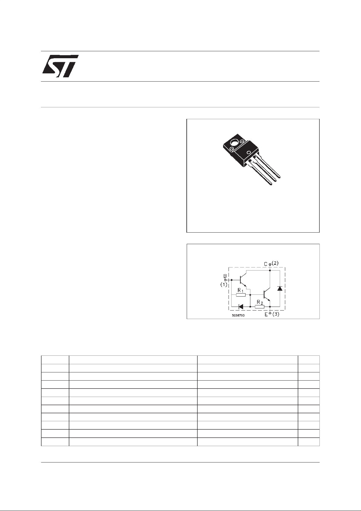
BU808DFP
NPN POWER DARLINGTON
3
2
1
APPLICATIONS
■ COST EFFECTIVESOLUTIONFOR
TO-220FP
HORIZONTAL DEFLECTIONIN LOW END
TV UP TO 21 INCHES.
DESCRIPTION
The BU808DFP is a NPN transistor in monolithic
Darlington configuration. It is manufactured using
INTERNAL SCHEMATIC DIAGRAM
Multiepitaxial Mesa technology for cost-effective
high performance.
ABSOLUTE MAXIMUM RATINGS
Symbol Parameter Value Unit
V
V
V
I
I
P
T
Collect or-Base Vol t age (IE= 0) 1400 V
CBO
Collect or-Emitte r V oltage (IB= 0) 700 V
CEO
Emitter-Base Voltag e (IC=0) 5 V
EBO
Collect or Current 8 A
I
C
Collect or Peak Cur rent (tp<5ms) 10 A
CM
Base Current 3 A
I
B
Base Pea k Curre nt (tp<5ms) 6 A
BM
Tot al Dissipa t io n at Tc=25oC42W
tot
Storage Temperature -65 to 150
stg
Max. Oper ating Junc t io n T e m pe r ature 150
T
j
o
C
o
C
June 2000
1/7

BU808DFP
THERMAL DATA
R
thj-case
Ther mal Resist ance Junctio n- ca s e M ax 2.98
o
C/W
ELECTRICAL CHARACTERISTICS (T
=25oC unlessotherwisespecified)
case
Symbol Parameter Test Cond itions Min. Typ. Max. Un it
I
CES
Collec t or Cut -off
Current (V
I
EBO
Emitt er Cut -of f Cu rrent
(I
∗ Collec t or -Emit t er
V
CE(sat)
C
=0)
BE
=0)
V
= 1400 V 400 µA
CE
V
=5V 100 mA
EB
IC=5A IB=0.5A 1.6 V
Saturation Voltage
∗ Base-Emi tter
V
BE(sat )
IC=5A IB=0.5A 2.1 V
Saturation Voltage
∗ DC Current Gain IC=5A VCE=5V
h
FE
INDUCTIVE LOAD
t
s
t
f
Storage Time
Fall Time
INDUCTIVE LOAD
t
V
∗
Pulsed: Pulse duration = 300 µs, duty cycle 1.5 %
Storage Time
s
t
Fall Time
f
Diode Forwa r d Volt ag e IF=5A 3 V
F
=5A VCE=5V Tj=100oC6020
I
C
VCC=150V IC=5A
=0.5A V
I
B1
VCC=150V IC=5A
=0.5A V
I
B1
=100oC
T
j
=-5V 3
BEo f f
=-5V
BEo f f
0.8
230
0.8
2
µs
µs
µs
µs
Safe Operating Area ThermalImpedance
2/7
BU808DFP
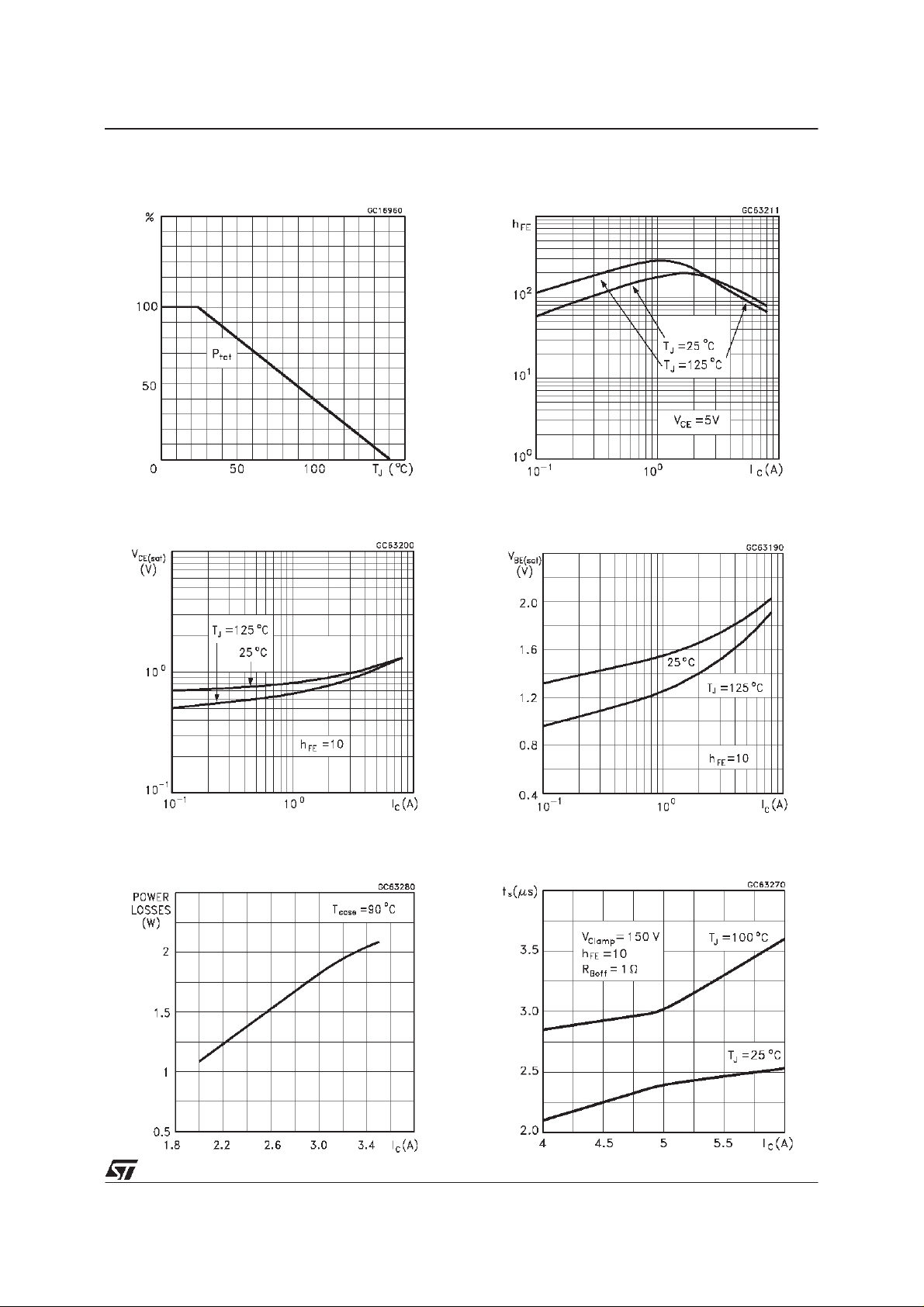
Derating Curve
CollectorEmitterSaturationVoltage
DC Current Gain
BaseEmitterSaturation Voltage
PowerLosses at 16 KHz
SwitchingTime InductiveLoad at 16KHz
3/7

BU808DFP
SwitchingTime InductiveLoad at 16KHZ ReverseBiasedSOA
BASEDRIVE INFORMATION
In order to saturate the power switch and reduce
conduction losses, adequate direct base current
has to be provided for the lowest gain hFEat
I
B1
o
100
C (line scan phase). On the other hand,
negative base current I
must be provided to
B2
turn off the power transistor (retrace phase).
Most of the dissipation, in the deflection
application, occurs at switch-off. Therefore it is
essential to determine the value of I
minimizes power losses, fall time t
consequently,T
defined to give total power losses, t
function of I
. A new set of curves have been
j
s
at both 16 KHz scanning
B2
which
B2
and,
f
and tfas a
frequencies for choosing the optimum negative
drive. The test circuit is illustratedin figure1.
Inductance L
serves to control the slope of the
1
negative base current I
excess carrier in the collector when base current
is still present, this would avoid any tailing
phenomenonin the collectorcurrent.
The values of L and C are calculated from the
followingequations:
1
L(I
2
C
)2=
1
2
C(V
CEfly
Where IC= operating collector current, V
flyback voltage, f= frequency of oscillation during
retrace.
to recombine the
B2
2
)
ω=2πf=
1
L
√
C
CEfly
=
4/7

Figure1: Inductive Load Switching TestCircuits.
Figure2: SwitchingWaveformsin a Deflection Circuit
BU808DFP
5/7

BU808DFP
TO-220FP MECHANICAL DATA
DIM.
MIN. TYP. MAX. MIN. TYP. MAX.
A 4.4 4.6 0.173 0.181
B 2.5 2.7 0.098 0.106
D 2.5 2.75 0.098 0.108
E 0.45 0.7 0.017 0.027
F 0.75 1 0.030 0.039
F1 1.15 1.7 0.045 0.067
F2 1.15 1.7 0.045 0.067
G 4.95 5.2 0.195 0.204
G1 2.4 2.7 0.094 0.106
H 10 10.4 0.393 0.409
L2 16 0.630
L3 28.6 30.6 1.126 1.204
L4 9.8 10.6 0.385 0.417
L6 15.9 16.4 0.626 0.645
L7 9 9.3 0.354 0.366
Ø 3 3.2 0.118 0.126
mm inch
E
A
D
B
L3
L6
L7
¯
F1
F
G1
H
G
F2
123
L2
L4
6/7

BU808DFP
Information furnished is believed to beaccurate and reliable. However, STMicroelectronics assumes no responsibility for the consequences
of use of such information nor for any infringement of patents or other rights of third parties which may result from its use. No license is
granted by implication or otherwise under any patent or patent rights of STMicroelectronics. Specification mentioned in this publication are
subject to change without notice. This publication supersedes and replaces all information previously supplied. STMicroelectronics products
are not authorized for use as critical components in life support devices or systems without express written approval of STMicroelectronics.
The ST logo is atrademark of STMicroelectronics
2000 STMicroelectronics – Printed in Italy – AllRights Reserved
STMicroelectronicsGROUP OF COMPANIES
Australia - Brazil - China - Finland- France - Germany - Hong Kong - India - Italy - Japan - Malaysia - Malta - Morocco -
Singapore-Spain - Sweden - Switzerland - United Kingdom - U.S.A.
http://www.st.com
7/7
 Loading...