

Datasheet BTB24-800B, BTB24-700B, BTB24-600B, BTB24-400B Datasheet (SGS Thomson Microelectronics)
®
FEATURES
HIGH SURGE CURRENT CAPABILITY
.
COMMUTATION : (dV/dt)c > 10V/µs
.
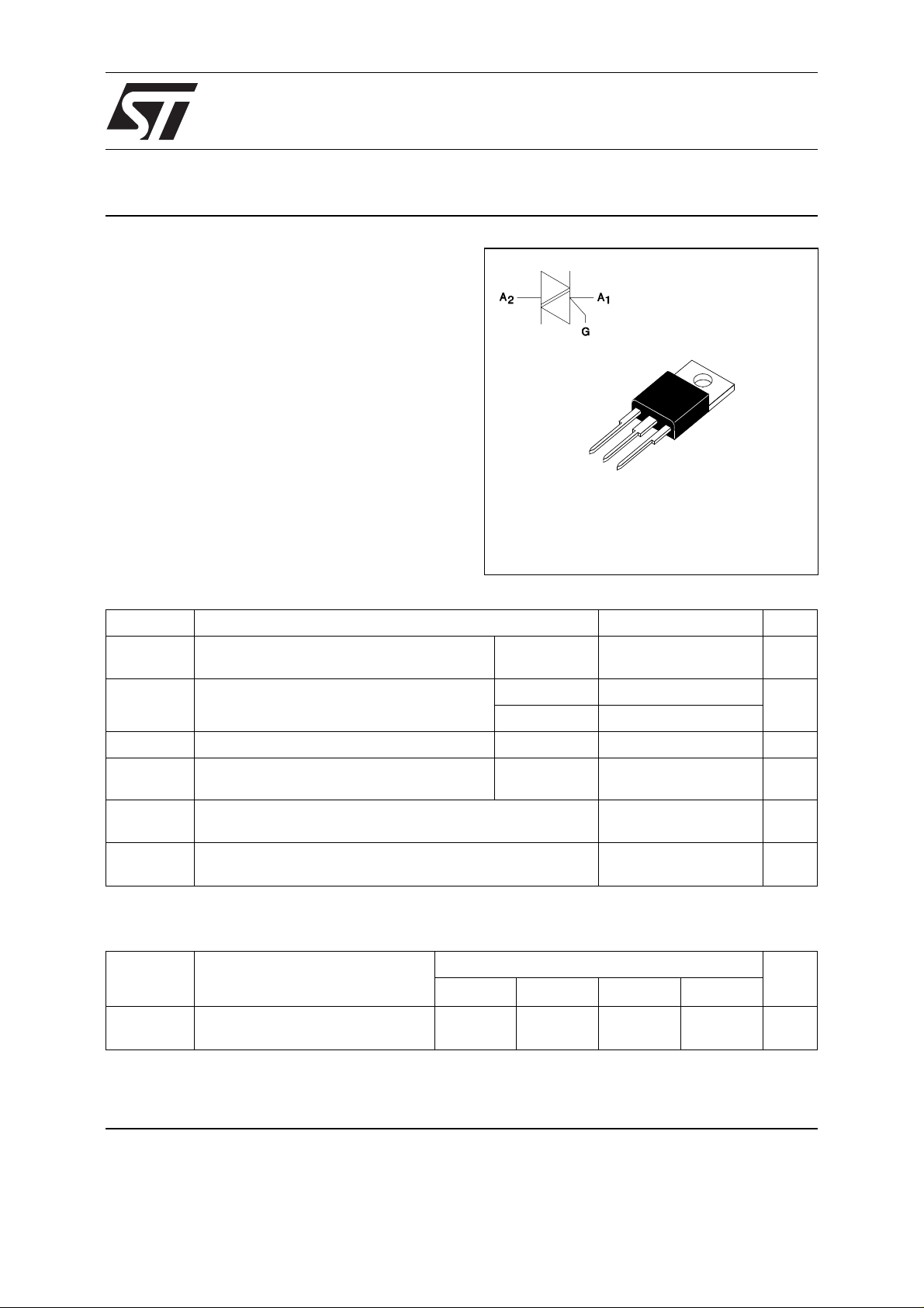
BTB24 B
STANDARD TRIACS
DESCRIPTION
The BTB24 B triac family are high performance
glass passivated PNPN devices.
These parts are suitables for general purpose applications where high surge current capability is required. Application such as phase control and
static switching on inductive or resistive load.
ABSOLUTE RATINGS
Symbol Parameter Value Unit
I
T(RMS)
I
TSM
I2tI
dI/dt Critical rate of rise of on-state current
Tstg
Tj
Tl Maximum lead temperature for soldering during 10 s at 4.5 mm
RMS on-state current
(360° conduction angle)
Non repetitive surge peak on-state current
( Tj initial = 25°C )
2
t value tp = 10 ms 312 A2s
Gate supply : IG = 2 . IGT tr ≤ 100ns
Storage and operating junction temperature range - 40 to + 150
from case
(limiting values)
Tc = 90 °C25 A
tp = 8.3 ms 260 A
tp = 10 ms 250
Repetitive
F = 100 Hz
A1
A2
G
TO220AB
(Plastic)
50 A/µ s
- 40 to + 125
260 ° C
°C
°C
Symbol Parameter BTB24-... B Unit
400 600 700 800
V
DRM
V
RRM
October 1998 - Ed: 2A
Repetitive peak off-state voltage
Tj = 125 °C
400 600 700 800 V
1/4
BTB24 B
THERMAL RESISTANCES
Symbol Parameter Value Unit
Rth (j-a) Junction to ambient 60 °C/W
Rth (j-c) DC Junction to case for DC 1.5 °C/W
Rth (j-c) AC Junction to case for 360° conduction angle ( F= 50 Hz) 1.1 °C/W
GATE CHARACTERISTICS
P
= 1W PGM = 10W (tp = 20 µs) IGM = 4A (tp = 20 µs) VGM = 16V (tp = 20 µs).
G (AV)
(maximum v alu es )
ELECTRICAL CHARACTERISTICS
Symbol Test Conditions Quadrant Suffix Unit
I
GT
V
GT
V
GD
I
L
IH *I
VTM *ITM= 35A tp= 380µs Tj=25°C MAX 1.6 V
I
DRM
I
RRM
dV/dt * Linear slope up to VD=67%V
(dV/dt)c * (dI/dt)c = 11.1A/ms Tj=125°C MIN 10 V/µs
* For either polarit y of electrode A2 voltage with reference to elec trode A1.
VD=12V (DC) RL=33Ω Tj=25°C I-II-III-IV MIN 5 mA
I-II-III MAX 50
IV MAX 100
VD=12V (DC) RL=33Ω Tj=25°C I-II-III-IV MAX 1.3 V
VD=V
IG=1.2 I
RL=3.3kΩ Tj=125°C I-II-III-IV MIN 0.2 V
DRM
GT
Tj=25°C I-III-IV MAX 70 mA
II 150
= 500mA gate open Tj=25°C MAX 50 m A
T
V
DRM
V
RRM
Rated
Rated
DRM
Tj=25°CMAX5µA
Tj=125°CMAX2mA
Tj=125°C MIN 750 V/µs
gate open
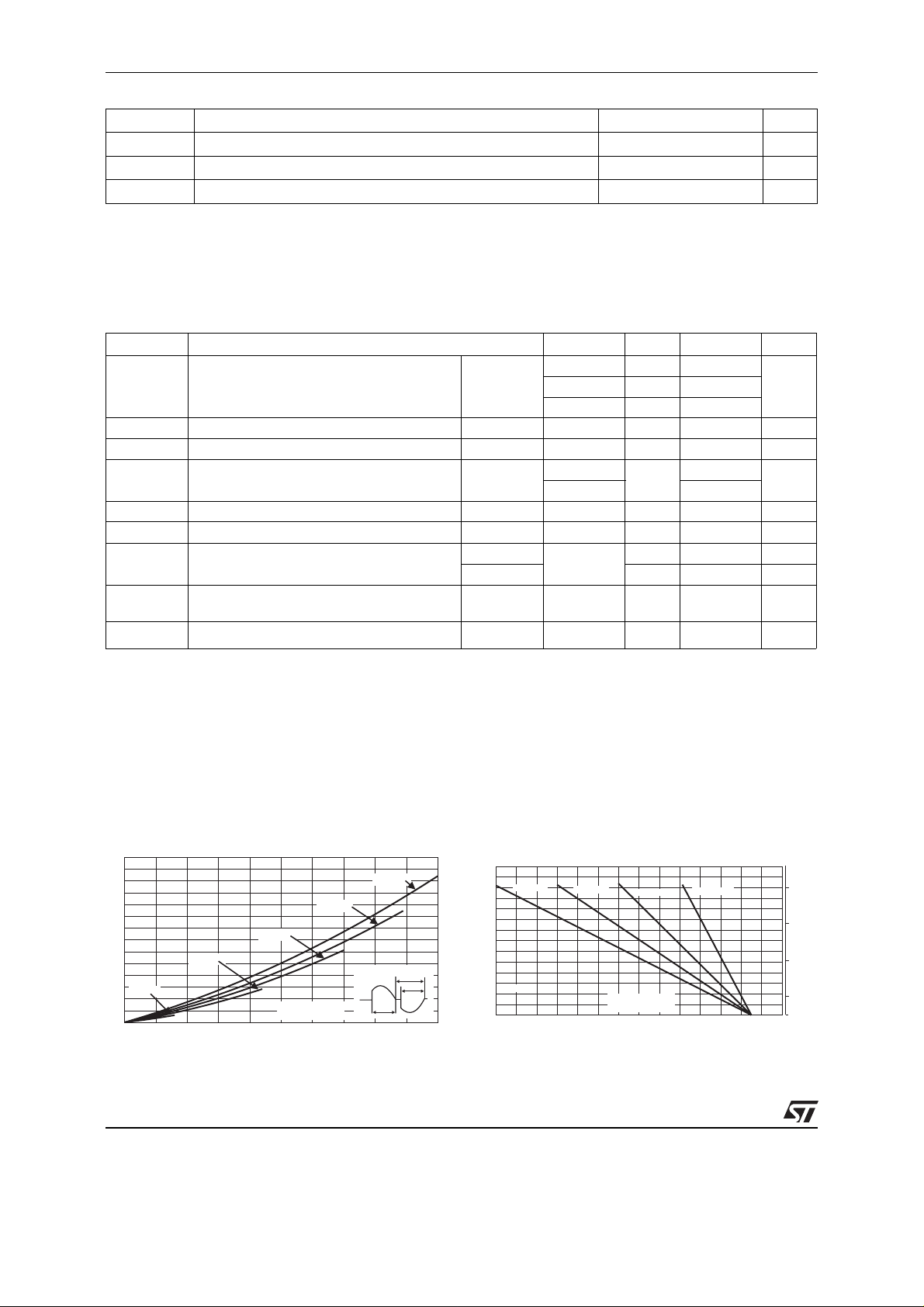
Fig. 1: Maximum power dissipation versus RMS
on-state current.
P(W)
35
30
25
20
15
α = 90°
α = 60°
α = 120°
10
α = 30°
5
0
0 5 10 15 20 25
IT(rms)(A)
α = 180°
α
180°
α
2/4
Fig. 2: Correlation between maximum power dissipation
and maximum allowable temperatures (T
T
) for different thermal resistances heatsink +
case
amb
and
contact.
Rth=0°C/W
Tcase (°C)
90
100
110
120
125
P(W)
35
Rth=3°C/W
30
25
20
15
10
α = 180°
5
0
0 20 40 60 80 100 120 140
Rth=2°C/W
Rth=1°C/W
Tamb(°C)
BTB24 B
Fig. 3: RMS on-state current versus case temperature.
IT(rms)(A)
30
α = 180°
25
20
15
10
5
Tcase(°C)
0
0 25 50 75 100 125
Fig. 5: Relative variation of gate trigger current and
holding current versus junction temperature (typical
values).
IGT,IH[Tj] / IGT,IH[Tj=25°C]
2.5
2.0
IGT
1.5
1.0
IH
0.5
Tj(°C)
0.0
-40 -20 0 20 40 60 80 100 120 140
Fig. 4: Relative variation of thermal impedance versus
pulse duration.
K=[Zth/Rth]
1.00
Zth(j-c)
0.10
Zth(j-a)
tp(s)
0.01
1E-3 1E-2 1E-1 1E+0 1E+1 1E+2 5E+2
Fig. 6: Non Repetitive surge peak on-state current
versus number of cycles.
ITSM(A)
220
200
180
160
140
120
100
80
60
40
20
0
1 10 100 1000
Number of cycles
Tj initial=25°C
F=50Hz
Fig. 7: Non repetitive surge peak on-state current for a
sinusoidal pulse with width : t ≤ 10ms, and
corresponding value of I2t.
ITSM(A),I²t(A²s)
1000
500
ITSM
I²t
200
tp(ms)
100
12 510
Tj initial=25°C
Fig. 8: On-state characteristics (maximum values).
ITM(A)
300
100
Tj=25°C
Tj=Tj max.
10
Tj max.:
Vto=0.95V
VTM(V)
1
0.0 0.5 1.0 1.5 2.0 2.5 3.0 3.5 4.0 4.5
Rt=19mΩ
3/4
BTB24 B
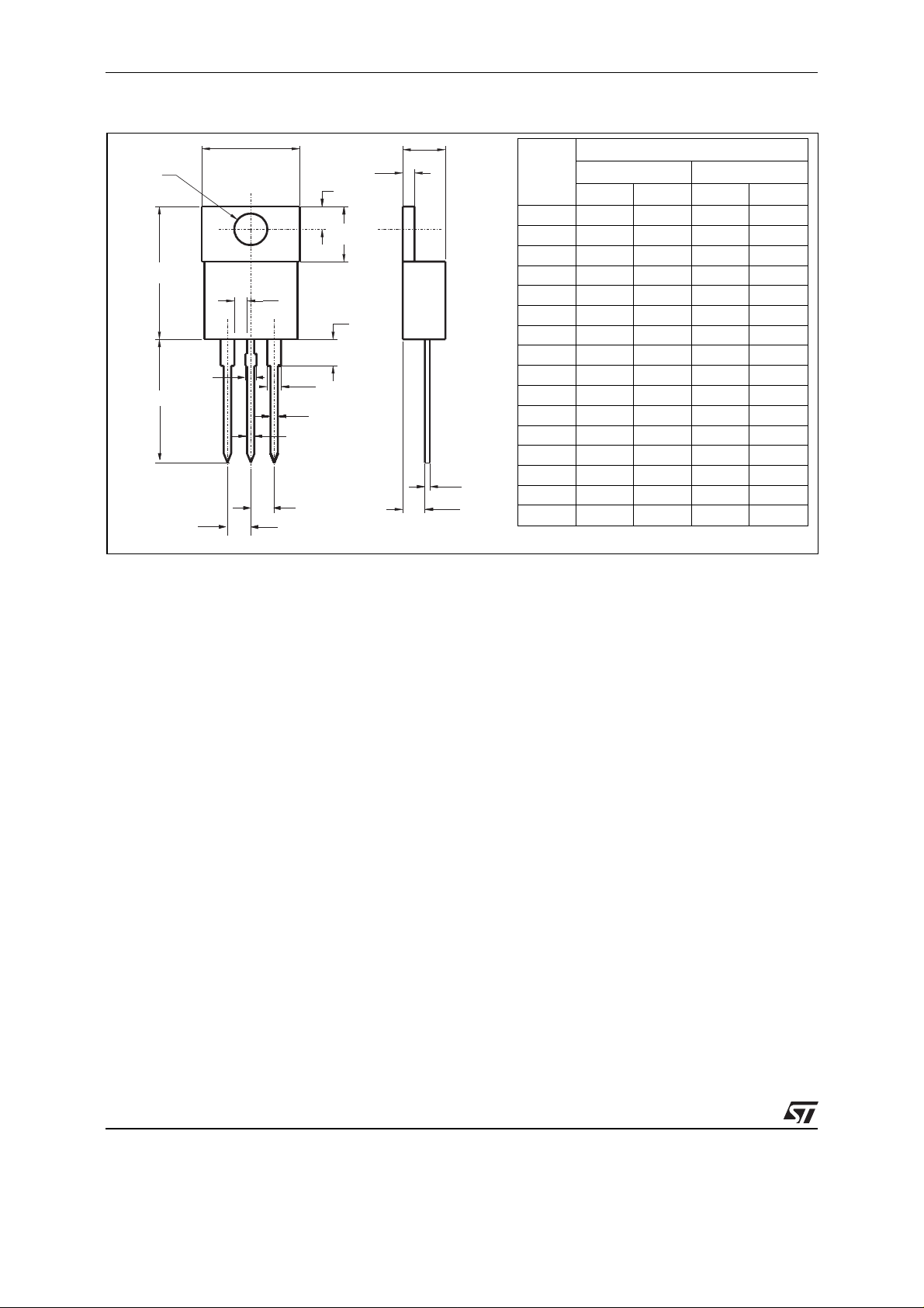
PACKAGE MECHANICAL DATA
TO220AB Plastic
B
I
L
A
l1
l3
a2
e
e
l2
b1
b1
C
b2
REF. DIMENSIONS
Millimeters Inches
Min. Max. Min. Max.
F
A 14.23 15.87 0.560 0.625
a1 4.50 0.177
a2 12.70 14.70 0.500 0.579
B 10.20 10.45 0.402 0.411
b1 0.64 0.96 0.025 0.038
a1
b2 1.15 1.39 0.045 0.055
C 4.48 4.82 0.176 0.190
c1 0.35 0.65 0.020 0.026
c2 2.10 2.70 0.083 0.106
e 2.29 2.79 0.090 0.110
F 5.85 6.85 0.230 0.270
I 3.55 4.00 0.140 0.157
L 2.54 3.00 0.100 0.118
c1
c2
I1 1.30 0.051
l2 1.45 1.75 0.057 0.069
l3 0.80 1.20 0.031 0.047
Cooling method : C
Marking : type number
Weight : 2.25 g
Recommended torque value : 0.8 m.N.
Maximum torque value : 1 m.N.
Information furnished is believed to be accurate and reliable. However, STMicroelectronics assumes no responsibility for the
consequences of use of such information nor for any infringement of patents or other rights of third parties which may result
from its use. No license is granted by implication or otherwise under any patent or patent rights of STMicroelectronics.
Specifications mentioned in this publication are subject to change wi thout notice. This publication supersedes and replaces
all information previously supplied. STMicroelectronics products are not authorized for use as critical components in life
support devices or systems without expr ess written approval of ST Microelectronics.
Austral ia - Brazi l - Canada - China - Fr ance - Germ any - Italy - Japan - K orea - Mala ysia - Malt a - Mexic o - Morocco -
The Net herlands - S ingapore - Spain - Swed en - Switz erland - Taiw an - Thai land - Unit ed Kingdom - U .S.A.
The ST logo is a regi stered tradem ark of STMicr oelectronics
© 1998 STM icroele ctronics - Printed i n Italy - All right s reser ved.
STMicroelectronics GROUP OF COMP ANIES
4/4
http://w w w. st .c om
 Loading...