

®
BTA/BTB12 and T12 Series
SNUBBERLESS™, LOGIC LEVEL & STANDARD 12A TRIACS
MAIN FEATURES:
Symbol Value Unit
I
T(RMS)
V
DRM/VRRM
I
GT (Q1)
12 A
600 and 800 V
10 to 50 mA
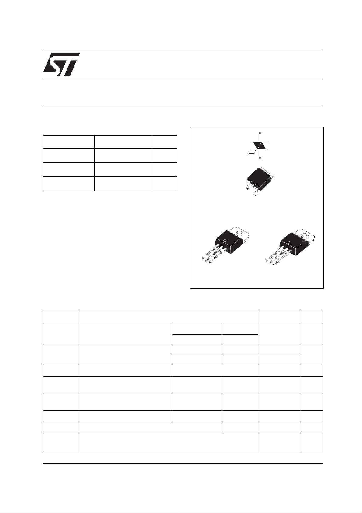
DESCRIPTION
Available either in through-hole or surface-mount
packages, the BTA/BTB12 and T1 2 triac series is
suitable for general purpose AC sw itching. They
can be used as an ON/OFF function in
applications such as static relays, heating
regulation, induction motor starting circuits... or for
phase control operation in light dimmers, motor
speed controllers,...
The snubberless versions (BTA/BTB...W and T12
series) are specially recommended for use on
inductive loads, than ks to their high com mutation
performances. By usin g an internal ceramic pa d,
the BTA series provides voltage insulated tab
(rated at 2500V RMS) complying with UL
standards (File ref.: E81734)
A1
A1
A2
G
TO-220AB Insulated
(BTA12)
A2
G
A1
A2
G
D2PAK
(T12-G)
A1
A2
A2
G
A2
TO-220AB
(BTB12)
ABSOLUTE MAXIMUM RATINGS
Symbol Parameter Value Unit
I
T(RMS)
I
TSM
²
I
dI/dt
V
DSM/VRSM
I
GM
P
G(AV)
T
stg
T
RMS on-state current (full sine wave)
Non repetitive surge peak on-state
current (full cycle, Tj initial = 25°C)
tI
²
t Value for fusing
Critical rate of rise of on-state current
I
= 2 x IGT , tr ≤ 100 ns
G
Non repetitive surge peak off-state
voltage
Peak gate current tp = 20 µs Tj = 125°C 4 A
Average gate power dissipation Tj = 125°C 1 W
Storage junction temperature range
Operating junction temp erature range
j
September 2000 - Ed: 3
²
PAK/TO-220AB
D
Tc = 105°C
12 A
TO-220AB Ins. Tc = 90°C
F = 50 Hz t = 20 ms 120 A
F = 60 Hz t = 16.7 ms 126
tp = 10 ms 100
F = 120 Hz Tj = 125°C 50 A/µs
V
tp = 10 ms Tj = 25°C
DRM/VRRM
+ 100
- 40 to + 150
- 40 to + 125
A
V
°C
²
s
1/7
BTA/BTB12 and T12 Series
ELECTRICAL CHARACTERISTICS (Tj = 25°C, unless otherwise specified)
■ SNUBBERLESS™ and LOGIC LEVEL (3 Quadrants)
Symbol Test Conditions Quadrant T 12 BTA/BTB12
T1235 SW CW BW
I
(1)
GT
V
V
GT
GD
= 12 V RL = 30 Ω
V
D
VD = V
RL = 3.3 kΩ
DRM
Tj = 125°C
I
(2)
H
I
L
dV/dt (2) V
= 100 mA
I
T
I
= 1.2 I
G
= 67 %V
D
GT
gate open
DRM
Tj = 125°C
(dI/dt)c (2) (dV/dt)c = 0.1 V/µs Tj = 125°C MIN. - 6.5 - - A/ms
(dV/dt)c = 10 V/µs Tj = 125°C - 2.9 - Without snubber Tj = 125°C 6.5 - 6.5 12
■ ST ANDARD (4 Quadrants)
Symbol Test Conditions Quadrant BTA/BTB06
I
(1)
GT
V
GT
V
GD
I
(2)
H
I
L
dV/dt (2) V
= 12 V RL = 30 Ω
V
D
VD = V
= 500 mA
I
T
IG = 1.2 I
= 67 %V
D
RL = 3.3 kΩ Tj = 125°C
DRM
GT
DRM
gate open Tj = 125°C
(dV/dt)c (2) (dI/dt)c = 5.3 A/ms Tj = 125°C MIN. 5 10 V/µs
I - II - III MAX. 35 10 35 50
I - II - III MAX. 1.3 V
I - II - III MIN. 0.2
MAX.35153550mA
I - III MAX. 50 25 50 70 mA
II 60 30 60 80
MIN. 500 40 500 1000 V/µs
CB
I - II - III
IV
MAX.
25
50
50
100
ALL MAX. 1.3 V
ALL MIN.
0.2 V
MAX. 25 50 mA
I - III - IV MAX. 40 50 mA
II 80 100
MIN. 200 400 V/µs
Unit
mA
V
Unit
mA
STATIC CHARACTERISTI CS
Symbol Test Conditions Value Unit
V
(2) ITM = 17 A tp = 380 µs
T
(2)
V
to
(2)
R
d
I
DRM
I
RRM
Note 1: minimum IGT is guaranted at 5% of IGT max.
Note 2: for both polarities of A2 referenced to A1
Threshold voltage Tj = 125°C MAX. 0.85 V
Dynamic resistance Tj = 125°C MAX. 35 mΩ
V
= V
DRM
RRM
2/7
Tj = 25°C MAX. 1.55 V
Tj = 25°C
Tj = 125°C 1 mA
MAX.
5µA
BTA/BTB12 and T12 Series
THERMAL RESISTANCES
Symbol Parameter Value Unit
R
th(j-c)
R
th(j-a)
S = Copper surface under tab
Junction to case (AC)
Junction to ambient
PRODUCT SELECTOR
S = 1 cm
²
²
PAK/TO-220AB
D
TO-220AB Insulated 2.3
D²PAK
TO-220AB
TO-220AB Insulated
1.4
45
60
°C/W
°C/W
Part Number
BTA/BTB12-xxxB X X 50 mA Standard TO-220AB
BTA/BTB12-xxxBW X X 50 mA Snubberless TO-220AB
BTA/BTB12-xxxC X X 25 mA Standard TO-220AB
BTA/BTB12-xxxCW X X 35 mA Snubberless TO-220AB
BTA/BTB12-xxxSW X X 10 mA Logic level TO-220AB
T1235-xxxG X X 35 mA Snubberless
BTB: non insulated TO-220AB package
Voltage (xxx)
Sensitivity Type
600 V 800 V
Package
²
D
PAK
ORDERING INFORMATION
BT A 12 - 600 BW
TRIAC
SERIES
SENSITIVITY &TYPE
INSULATION:
A: insulated
B: non insulated
CURRENT:12A
VOLTAGE:
600: 600V
800: 800V
B: 50mA STANDARD
BW: 50mA SNUBBERLESS
C: 25mA STANDARD
CW: 35mA SNUBBERLESS
SW: 10mA LOGIC LEVEL
TRIAC
SERIES
CURRENT:12A
T 12 35 - 600 G (-TR)
PACKAGE:
2
G: D PAK
VOLTAGE:
600: 600V
800: 800V
SENSITIVITY:
35: 35mA
PACKING MODE:
Blank:Tube
-TR:Tape & Reel
3/7

BTA/BTB12 and T12 Series
OTHER INFORMATION
Part Number Marking Weight
Base
quantity
Packing
mode
BTA/BTB12-xxxyz BTA/BTB12-xxxyz 2.3 g 250 Bulk
T1235-xxxG T1235xxxG 1.5 g 50 Tube
T1235-xxxG-TR T1235xxxG 1.5 g 1000 Tape & reel
Note: xxx = voltage, yy = sensitivity, z = type
Fig. 1: Maximum power dissipation versus RMS
on-state current (full cycle).
P (W)
6
4
2
0
8
6
4
2
0
0123456789101112
IT(RMS)(A)
Fig. 2-1: RMS on-state current versus case
temperature (full cycle).
IT(RMS) (A)
14
13
12
11
10
9
8
7
6
5
4
3
2
1
0
0 25 50 75 100 125
Tc(°C)
BTB/T12
BTA
Fig. 2-2: RMS on-state current versus ambient
temperature (printed circuit board FR4, copper
thickness: 35µm),full cycle.
IT(RMS) (A)
3.5
3.0
2.5
2.0
1.5
1.0
0.5
0.0
0 25 50 75 100 125
Tamb(°C)
2
DPAK
(S=1cm )
2
Fig. 3: Relative variation of thermal impedance
versus pulse duration.
K=[Zth/Rth]
1E+0
Zth(j-c)
1E-1
1E-2
1E-3 1E-2 1E-1 1E+0 1E+1 1E+2 5E+2
Zth(j-a)
tp(s)
4/7

BTA/BTB12 and T12 Series
Fig. 4: On-state characteristics (maximum
values).
ITM (A)
100
Tj max
10
1
0.5 1.0 1.5 2.0 2.5 3.0 3.5 4.0 4.5 5.0
Tj=25°C
VTM(V)
Tj max.
Vto = 0.85 V
Rd = 35 m
Ω
Fig. 6: Non-repetitive surge peak on-state
current for a sinusoidal pulse with width
tp < 10ms, and corresponding value of I²t.
ITSM (A), I²t (A²s)
1000
100
dI/dt limitation:
50A/µs
Tj initial=25°C
ITSM
I²t
Fig. 5: Surge peak on-state current versus
number of cycles.
ITSM (A)
130
120
110
100
90
80
Non repetitive
Tj initial=25°C
t=20ms
One cycle
70
60
50
40
Repetitive
Tc=90°C
30
20
10
0
1 10 100 1000
Number of cycles
Fig. 7: Relative variation of gate trigger current,
holding current and latching current versus
junction temperature (typical values).
IGT,IH,IL[Tj] / IGT,IH,IL [Tj=25°C]
2.5
2.0
1.5
1.0
IGT
IH & IL
tp (ms)
10
0.01 0.10 1.00 10.00
Fig. 8: Relative variation of critical rate of
decrease of main current versus (dV/dt)c (typical
values).
(dI/dt)c [(dV/dt)c] / Specified (dI/dt)c
2.8
SW
2.4
2.0
C
1.6
B
1.2
0.8
0.4
0.0
0.1 1.0 10.0 100.0
(dV/dt)c (V/µs)
BW/CW/T1235
0.5
Tj(°C)
0.0
-40 -20 0 20 40 60 80 100 120 140
Fig. 9: Relative variation of critical rate of
decrease of main current versus junction
temperature.
(dI/dt)c [Tj] / (dI/dt)c [Tj specified]
6
5
4
3
2
1
0
0 25 50 75 100 125
Tj (°C)
5/7

BTA/BTB12 and T12 Series
Fig. 10: D²PAK Thermal resistance junction to
ambient versus copper surface under tab (printed
circuit board FR4, copper thickness: 35 µm).
Rth(j-a) (°C/W)
80
70
60
50
40
30
20
10
0
0 4 8 1216202428323640
S(cm²)
PACKAGE MECHANICAL DATA
D²PAK (Plastic)
D²PAK
DIMENSIONS
A
L2
L
L3
E
B2
B
G
2.0 MIN.
FLAT ZONE
C2
A1
C
A2
FOOTPRINT DIMENSIONS (in millimete r s )
D²PAK (Plastic)
16.90
R
V2
REF .
Millimeters Inches
Min. Typ. Max. Min. Typ. Max.
A 4.30 4.60 0.169 0.181
A1 2.49 2.69 0.098 0.106
D
A2 0.03 0.23 0.001 0.009
B 0.70 0.93 0.027 0.037
B2 1.25 1.40 0.048 0.055
C 0.45 0.60 0.017 0.024
C2 1.21 1.36 0.047 0.054
D 8.95 9.35 0.352 0.368
E 10.00 10.28 0.393 0.405
G 4.88 5.28 0.192 0.208
L 15.00 15.85 0.590 0.624
L2 1.27 1.40 0.050 0.055
L3 1.40 1.75 0.055 0.069
R 0.40 0.016
V2 0° 8° 0° 8°
6/7
10.30
8.90
5.08
1.30
3.70

PACKAGE MECHANICAL DATA
TO-220 AB / TO-220AB Ins.
B
L
I
A
l4
a1
l3
l2
a2
b1
e
BTA/BTB12 and T12 Series
DIMENSIONS
C
b2
REF.
A 15.20 15.90 0.598 0.625
F
a1 3.75 0.147
a2 13.00 14.00 0.511 0.551
B 10.00 10.40 0.393 0.409
b1 0.61 0.88 0.024 0.034
b2 1.23 1.32 0.048 0.051
C 4.40 4.60 0.173 0.181
c2
c1 0.49 0.70 0.019 0.027
c2 2.40 2.72 0.094 0.107
e 2.40 2.70 0.094 0.106
F 6.20 6.60 0.244 0.259
I 3.75 3.85 0.147 0.151
I4 15.80 16.40 16.80 0.622 0.646 0.661
M
c1
L 2.65 2.95 0.104 0.116
l2 1.14 1.70 0.044 0.066
l3 1.14 1.70 0.044 0.066
M 2.60 0.102
Millimeters Inches
Min. Typ. Max. Min. Typ. Max.
Information furnished is believed to be accurate and reliable. However, STMicroelectronics assumes no responsibility for the consequences
of use of su ch in for mat i on n or f or a ny in fr ing em ent of pa te nts or o ther r igh ts of th ir d pa r tie s w hic h may res ul t f rom i ts us e. No license is granted
by impl i cation or otherwise under any p at ent or patent rights of STMicroelectronic s. S pecificat i ons mentioned in this publication are subje ct
to change wi t hout notice. Thi s publication supersede s and replaces all in formation prev i ously supplied. STMicroel ectronics products are not
authori zed for use as cr i tical components in life sup port devices or systems wit hout express w ri tten approval of STMicroelectronics.
© The ST logo is a registered trademark of STMicroelectronics
© 2000 STMicroelectronics - Printed in Italy - All Rights Reserved
STMicroele ct ronics GROUP OF COM P A NI E S
Australi a - Brazil - China - Finland - F rance - Germany - Hong Kon g - India - Italy - Japan - Malaysi a - Malta - Morocco
Singapo re - Spain - Swe den - Switze rl and - United K i ngdom
http://www.st.co m
7/7
 Loading...