

®
SILICON POWER DARLINGTON TRANSISTOR
APPLICATIONS:
■ GENERAL PURPO SE SWITCHING AND
AMPLIFIER
■ LINEAR AND SWITCHING INDUSTRIAL
EQUIPMENT
■ FULLY INSULAT E D PACKA G E (U.L.
COMPLIANT) FOR EASY MOUNTING
DESCRIPTION
The BDX53BFP is a silicon Epitaxial-Base NPN
power transistor in monolithic Darlington
configuration mounted in T0-220FP fully molded
isolated package. It is intented for use in hammer
drivers, audio amplifiers and other medium power
linear and switching applications.
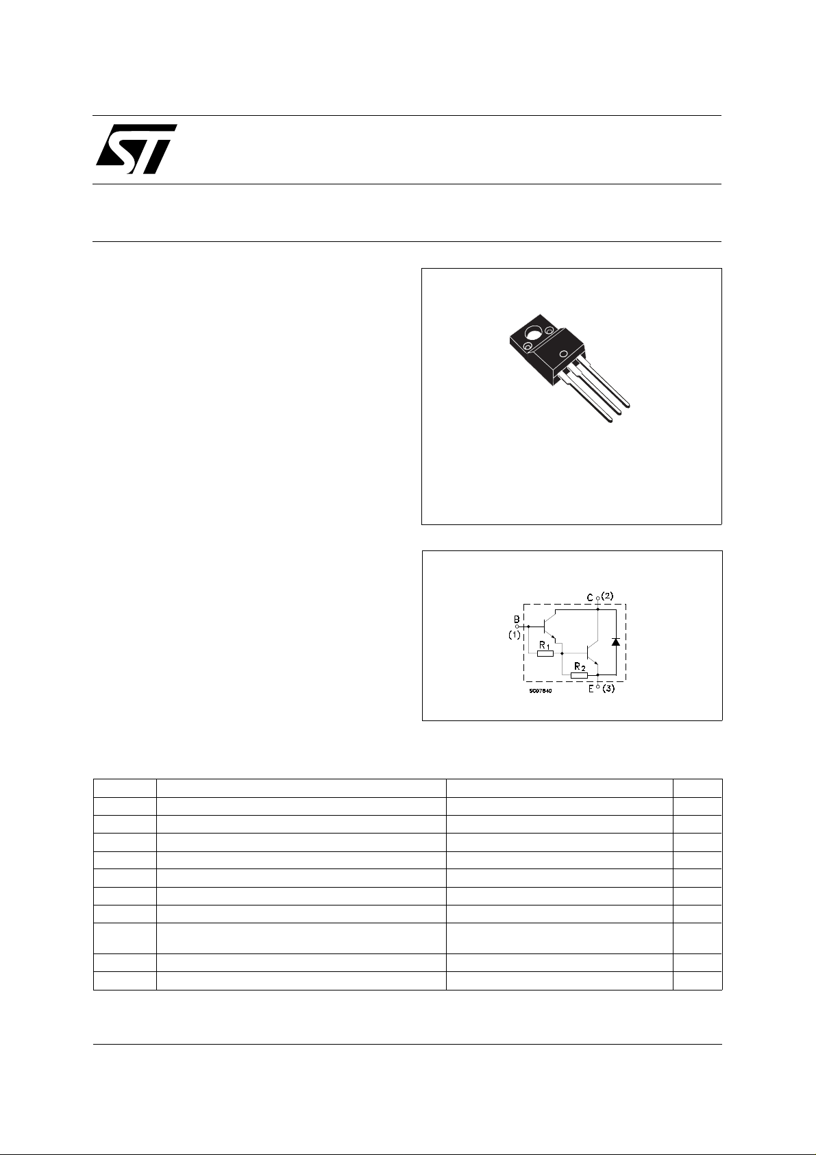
BDX53BFP
3
2
1
T0-220FP
INTER NAL SCH E M ATI C DIAG RA M
R1 Typ. = 10 KΩ R2 Typ. = 150 Ω
ABSOLUTE MAXIMUM RATINGS
Symbol Parameter Value Unit
V
V
V
I
P
V
T
Collector-Base Voltage (IE = 0) 80 V
CBO
Collector-Emitter Voltage (IB = 0) 80 V
CEO
Emitter-base Voltage (IC = 0) 5 V
EBO
I
Collector Current 8 A
C
Collector Peak Current (repetitive) 12 A
CM
Base Current 0.2 A
I
B
Total Dissipation at Tc ≤ 25 oC
tot
Insulation Withstand Voltage (RMS) from All
isol
29 W
1500 V
Three Leads to External Heatsink
Storage Temperature -65 to 150
stg
T
Max. Operating Junction Temperature 150
j
o
C
o
C
February 2003
1/4
BDX53BF P
THERMAL DATA
R
thj-case
R
thj-amb
Thermal Resistance Junction-case Max
Thermal Resistance Junction-ambient Max
4.3
70
o
C/W
o
C/W
ELECTRICAL CHARACTERISTICS (T
= 25 oC unless otherwise specified)
case
Symbol Parameter Test Conditions Min. Typ. Max. Unit
I
CBO
I
CEO
I
EBO
V
CEO(sus)
Collector Cut-off
Current (I
= 0)
E
Collector Cut-off
Current (I
= 0)
B
Emitter Cut-off Current
(I
= 0)
C
∗ Collector-Emitter
= 80 V 0.2 mA
V
CB
= 40 V 0.5 mA
V
CE
V
EB
= 5 V
2mA
I
= 100 mA 80 V
C
Sustaining Voltage
(I
= 0)
B
∗ Collector-emitter
V
CE(sat)
IC = 3 A IB =12 mA 2 V
Saturation Voltage
V
∗ Base-emitter
BE(sat)
IC = 3 A IB =12 mA 2.5 V
Saturation Voltage
∗ DC Current Gain IC = 3 A VCE = 3 V 750
h
FE
VF∗ Parallel Diode Forward
Voltage
∗ Pulsed: Pulse duration = 300 µs, duty cycle 1.5 %
IF = 3 A
I
= 8 A
F
1.8
2.5
2.5 V
V
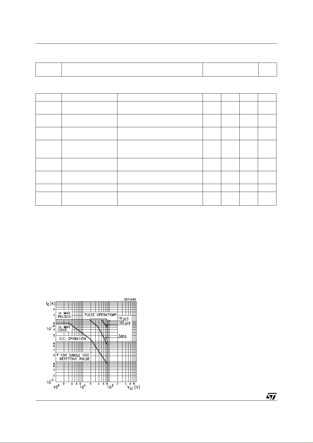
Safe Operating Are a
2/4

TO-220FP MECHANICAL DATA
BDX53BFP
DIM.
MIN. TYP. MAX. MIN. TYP. MAX.
A 4.4 4.6 0.173 0.181
B 2.5 2.7 0.098 0.106
D 2.5 2.75 0.098 0.108
E 0.45 0.7 0.017 0.027
F 0.75 1 0.030 0.039
F1 1.15 1.7 0.045 0.067
F2 1.15 1.7 0.045 0.067
G 4.95 5.2 0.195 0.204
G1 2.4 2.7 0.094 0.106
H 10 10.4 0.393 0.409
L2 16 0.630
L3 28.6 30.6 1.126 1.204
L4 9.8 10.6 0.385 0.417
L6 15.9 16.4 0.626 0.645
L7 9 9.3 0.354 0.366
Ø 3 3.2 0.118 0.126
mm inch
A
B
H
E
D
L3
L6
L7
¯
F1
F
G1
G
F2
123
L2
L4
3/4

BDX53BF P
Information furnished is believed to be accurate and reliable. However, STMicroelectronics assumes no responsibility for the consequences
of use of such inform ation nor for any infringe ment o f patents or other rig hts o f third par ties which ma y resul t from i ts use. N o li cen se is
granted by implicatio n or otherwise under any patent or patent rights of STMicroelectronics. Specification mentioned in this publication are
subject to change without notice. This publication supersedes and replaces all information previously supplied. STMicroelectronics products
are not authorized for use as critical compo nents in life support devices or systems without express written approval of STMicroelectronics.
The ST logo is a trademark of STMicroelectronics
© 2003 STMicroelectro nics – Printed in Italy – All Rights Reserved
STMicroelectronics GROUP OF COMPANIES
Australia - Brazil - Canada - China - Finland - France - Germany - Hong Kong - India - Israel - Italy - Japan - Malaysia - Malta - Morocco -
Singapore - Spain - Sweden - Switzerland - United Kingdom - United States.
http://www.st.com
4/4
 Loading...