

BDX33B BDX33C
COMPLEMENTARY SILICON POWER
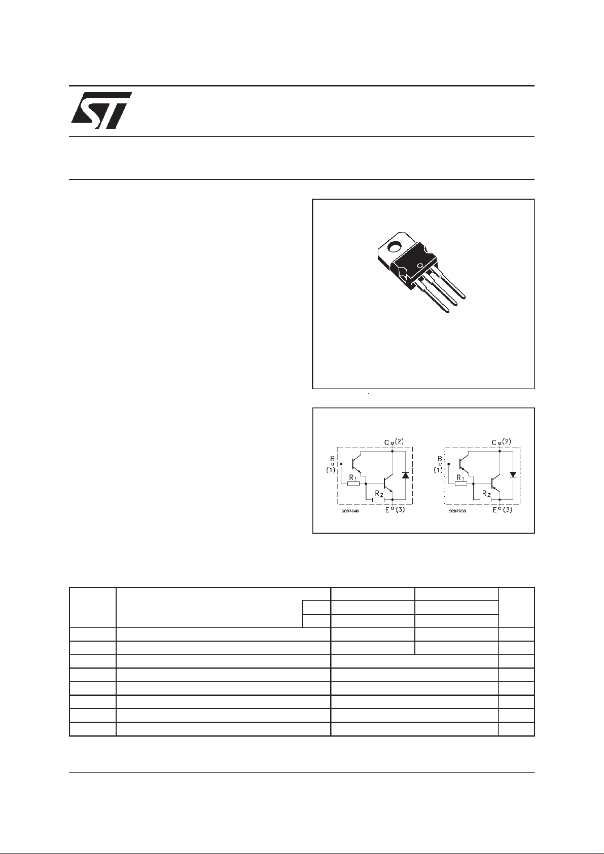
DESCRIPTION
The BDX33B and BDX33C are silicon
Epitaxial-Base NPN power transistors in
monolithic Darlington configuration mounted in
Jedec TO-220 plasticpackage. They are intented
for use in power linear and switching applications.
The complementary PNP types are BDX34Band
BDX34Crespectively.
BDX34B BDX34C
DARLINGTON TRANSISTORS
3
2
1
TO-220
INTERNAL SCHEMATIC DIAGRAM
R1Typ. = 10 KΩ R2Typ. = 150 Ω
ABSOLUTE MAXIMUM RATINGS
Symbol Parameter Unit
NPN BDX33 B BDX 33C
PNP BDX34B BDX34C
V
V
I
P
T
For PNP types voltage andcurrentvalues are negative.
Collec t or -Base Voltage (IE= 0 ) 80 100 V
CBO
Collec t or -Emitter Voltage (IB= 0) 80 100 V
CEO
Collector Current 10 A
I
C
Collector Peak Current 15 A
CM
Base Current 0.25 A
I
B
Tot al Dissipat ion at Tc≤ 25 oC
tot
St orage Tempe rat ure -65 t o 150
stg
Max. O perating Junction Temperat ure 150
T
j
70 W
o
C
o
C
October 1999
1/4
BDX33B BDX33CBDX34B BDX34C
THERMAL DATA
R
thj-case
Ther mal Resist anc e Junc t ion-case 1.78
o
C/W
ELECTRICAL CHARACTERISTICS
=25oC unless otherwisespecified)
(T
case
Symbol Parameter Test Condi tions Mi n. Typ . Max. U n it
I
CBO
I
CEO
I
EBO
V
CEO(sus)
V
CER(sus)
V
CEV(su s)
V
CE(sat)
Collect o r Cut- off Curr ent
=0)
(I
E
Collect o r Cut- off Curr ent
(I
=0)
B
Emitter Cut-off Current
=0)
(I
C
Collector-Emitter Sustaining
∗
Voltage ( I
Collect o r- emit ter Sust aining
∗
Voltage ( R
B
=0)
BE
=100 Ω)
∗ Collect or-emitter Sust ain ing
Voltage ( V
=-1.5 V)
BE
∗ Collecto r- emit ter Sat uration
BDX33B/ 3 4B
for
for BDX33C/34C V
= 100oC
T
case
for BDX33B/34B V
BDX33C /3 4C VCB=100V
for
BDX33B/ 3 4B
for
for BDX33C/34C V
= 100oC
T
case
for BDX33B/34B V
BDX33C/ 3 4C
for
V
=5V 5 mA
EB
I
=100 mA for BD X 33B /3 4B
C
V
V
V
CB
CB
=80V
CB
CE
CE
CE
CE
=80V
= 100V
=40V
= 50V
=40V
=50V
for B DX33C/34C80100
I
= 100 mA fo r BDX33 B/ 34B
C
I
= 100 mA fo r BDX33B /3 4B
C
BDX33C/ 3 4C
for
BDX33C/34C
for
80
100
80
100
IC=3A IB=6mA 2.5 V
0.2
0.2
5
5
0.5
0.5
10
10
Voltage
V
h
BE
FE
V
Base- emitter V ol t age I
∗
∗ DC Current G ain IC=3A VCE= 3 V 750 V
∗ Parallel-Diode Forwar d
F
=3A VCE=3V 2.5 V
C
IF=8A 4 V
Voltage
h
∗
Pulsed: Pulse duration = 300 µs, duty cycle 1.5 %
For PNP types voltage and current values are negative.
SmallSignalCurrentGain IC=1A VCE=5V f=1MHz 100
fe
mA
mA
mA
mA
mA
mA
mA
mA
V
V
V
V
V
V
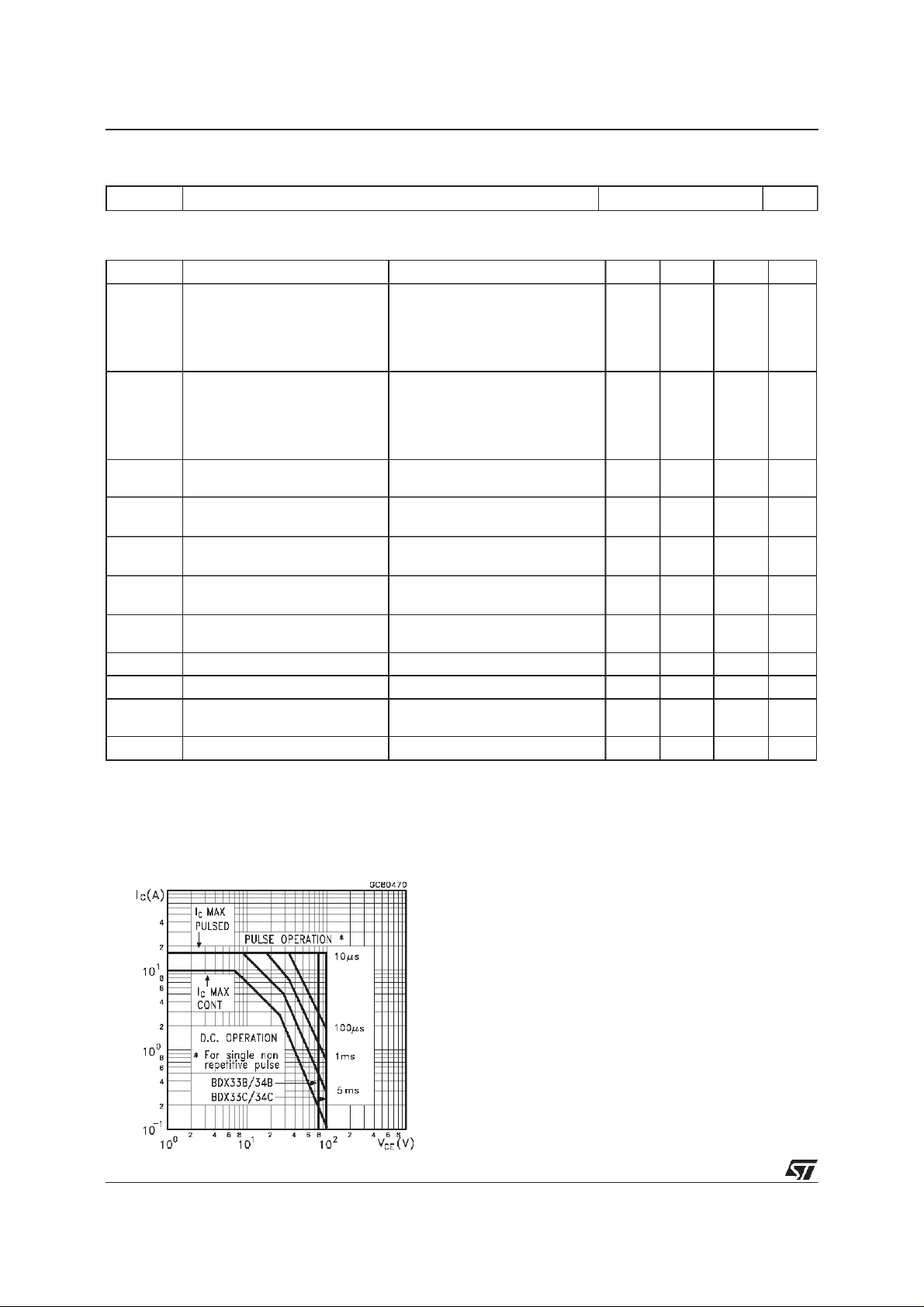
SafeOperatingArea
2/4
BDX33B BDX33C BDX34B BDX34C
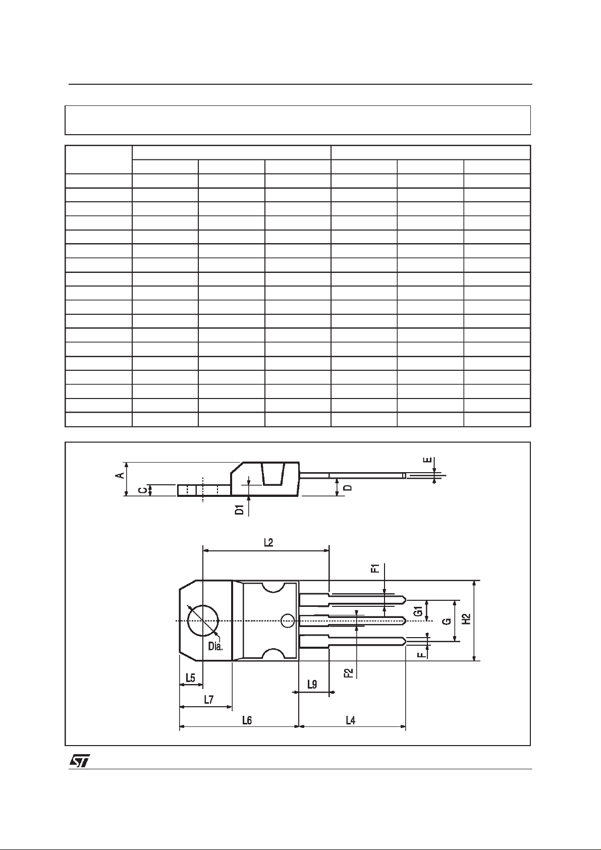
TO-220 MECHANICAL DATA
DIM.
MIN. TYP. MAX. MIN. TYP. MAX.
A 4.40 4.60 0.173 0.181
C 1.23 1.32 0.048 0.051
D 2.40 2.72 0.094 0.107
D1 1.27 0.050
E 0.49 0.70 0.019 0.027
F 0.61 0.88 0.024 0.034
F1 1.14 1.70 0.044 0.067
F2 1.14 1.70 0.044 0.067
G 4.95 5.15 0.194 0.203
G1 2.4 2.7 0.094 0.106
H2 10.0 10.40 0.393 0.409
L2 16.4 0.645
L4 13.0 14.0 0.511 0.551
L5 2.65 2.95 0.104 0.116
L6 15.25 15.75 0.600 0.620
L7 6.2 6.6 0.244 0.260
L9 3.5 3.93 0.137 0.154
DIA. 3.75 3.85 0.147 0.151
mm inch
P011C
3/4

BDX33B BDX33CBDX34B BDX34C
Information furnished is believed to be accurate and reliable. However, STMicroelectronics assumes no responsibility forthe consequences
of use of such information nor for any infringement of patents or other rights of third parties which may result from its use. No license is
granted by implicationor otherwise under any patent or patent rights of STMicroelectronics. Specification mentioned in this publication are
subject to change without notice. This publication supersedes and replaces all information previously supplied. STMicroelectronics products
are not authorized for use as critical components in life support devices or systems without express written approval of STMicroelectronics.
The ST logo is a trademarkof STMicroelectronics
1999 STMicroelectronics – Printed in Italy – All Rights Reserved
STMicroelectronics GROUP OF COMPANIES
Australia - Brazil -China - Finland - France - Germany - Hong Kong - India - Italy - Japan - Malaysia - Malta - Morocco -
Singapore - Spain - Sweden - Switzerland - United Kingdom - U.S.A.
http://www.st.com
.
4/4
 Loading...