


BAR 42
SMALLSIGNAL SCHOTTKY DIODES
DESCRIPTION
General purposemetal to silicon diodes featuring
very low turn-onvoltageand fastswitching.
BAR 43, A, C, S
K
N.C.
A
BAR42/BAR43 BAR43A
K
A1
A2
BAR43C BAR43S
A
A1
K2
A2
K1
K2
K1
SOT-23
(Plastic)
ABSOLUTERATINGS (limiting values)
Symbol Parameter Value Unit
V
RRM
I
FSM
P
T
I
stg
Repetitivepeak reversevoltage 30 V
Continuousforwardcurrent 100 mA
F
Surge non repetitiveforwardcurrent tp=10mssinusoidal 750 mA
Power dissipation (note 1) T
tot
=25°C 250 mW
amb
Maximumstorage temperaturerange - 65to +150
Tj Maximumoperating junction temperature* 150
T
Note 1: for double diodes,Ptot is the total power dissipation of both diodes.
dPtot
*:
Maximumtemperaturefor soldering during 10s 260
L
1
dTj
<
Rth(j−a
thermal runaway conditionfor a diode on itsown heatsink
)
THERMAL RESISTANCE
Symbol Testconditions Value Unit
R
th(j-a)
* Mounted on epoxy boardwith recommended padlayout.
Junction-ambient* 500
°C/W
°
°C
°C
C
June 1999- Ed: 2A
1/4
BAR 42/BAR 43, A, C, S
ELECTRICALCHARACTERISTICS
STATIC CHARACTERISTICS
Symbol TestConditions Min. Typ. Max. Unit
V
BR
V
F
**
I
R
Tj = 25°CI
*
Tj = 25°C
Tj = 25°C
= 100µA
R
BAR 42 IF= 10 mA 0.35 0.4 V
= 50 mA 0.5 0.65
I
F
BAR 43 I
All I
= 2 mA 0.26 0.33
F
= 15 mA 0.45
I
F
= 100 mA 1
F
VR=25V 500 nA
Tj = 100°C 100
Pulse test: * tp = 380µs,δ<2%
** tp= 5ms,δ<2%
DYNAMICCHARACTERISTICS
Symbol TestConditions Min. Typ. Max. Unit
C
trr Tj = 25°CI
η*Tj=25°CR
* Detectionefficiency.
Tj = 25°CV
=1mA RL= 100Ω
I
rr
F = 45Mhz V
=1V F = 1MHz
R
=10mA IR=10mA
F
=50KΩ CL= 300 pF
L
= 2V forBAR 43
i
30 V
7pF
5ns
80 %
A
µ
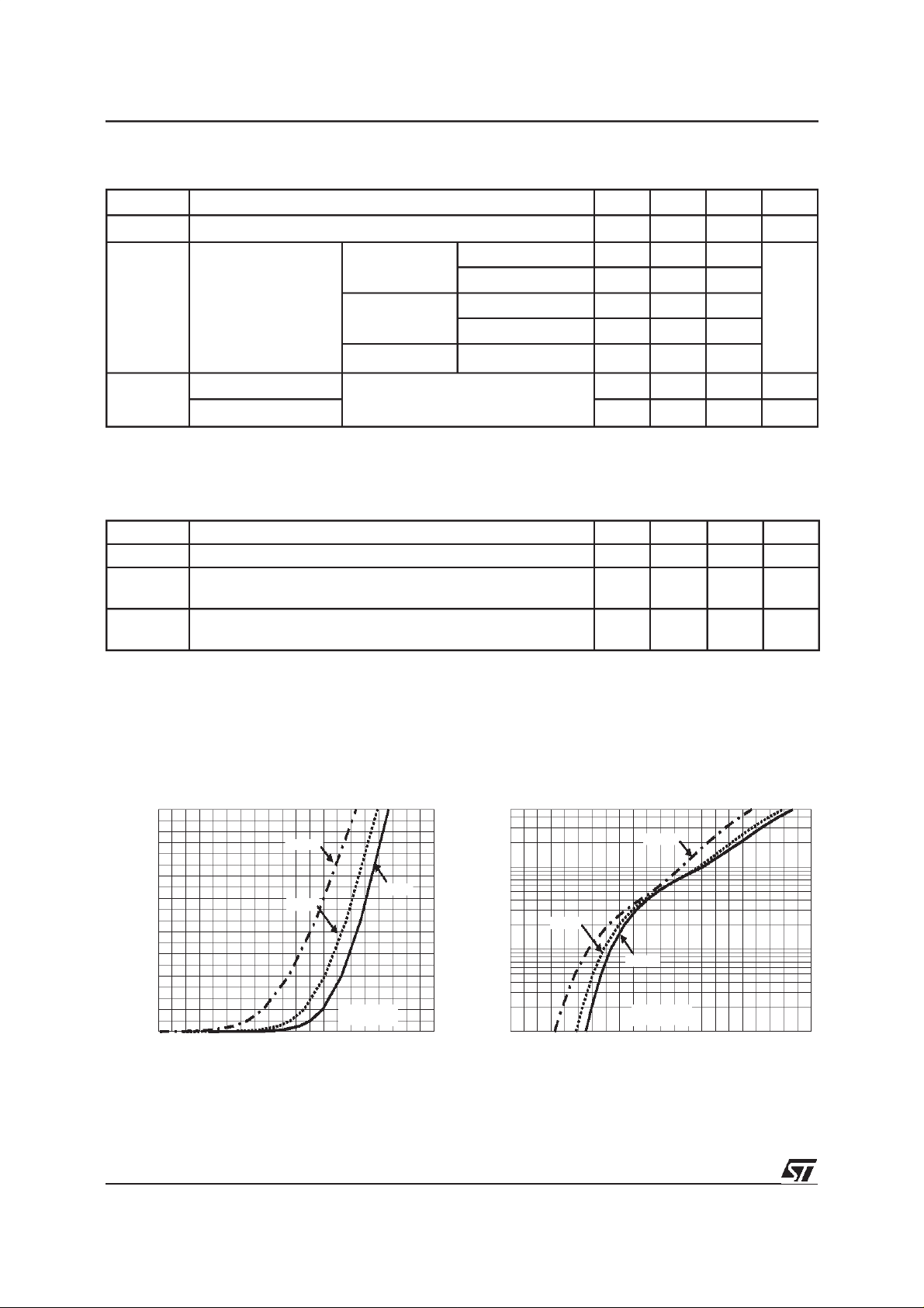
Fig. 1-1: Forward voltage drop versus forward
current(typicalvalues, low level).
IFM(A)
2.00E-2
1.80E-2
1.60E-2
1.40E-2
1.20E-2
1.00E-2
8.00E-3
6.00E-3
4.00E-3
2.00E-3
0.00E+0
0.00 0.05 0.10 0.15 0.20 0.25 0.30 0.35 0.40 0.45 0.50
Tj=100°C
Tj=25°C
Tj=50°C
VFM(V)
2/4
Fig. 1-2: Forward voltage drop versus forward
current(typicalvalues, high level).
IFM(A)
5E-1
Tj=100°C
1E-1
Tj=50°C
1E-2
1E-3
0.0 0.1 0.2 0.3 0.4 0.5 0.6 0.7 0.8 0.9 1.0 1.1
Tj=25°C
VFM(V)

BAR42/BAR 43, A, C, S
Fig. 2: Reverse leakage current versus reverse
voltageapplied (typicalvalues).
IR(µA)
1E+2
Tj=100°C
1E+1
1E+0
1E-1
Tj=50°C
Tj=25°C
VR(V)
1E-2
0 5 10 15 20 25 30
Fig . 4: Junction capacitance versus reverse
voltageapplied(typical values).
C(pF)
10
F=1MHz
Tj=25°C
Fig. 3: Reverse leakage current versus junction
temperature.
IR(µA)
1E+4
VR=30V
1E+3
1E+2
1E+1
1E+0
1E-1
Tj(°C)
1E-2
0 25 50 75 100 125 150
Fig. 5: Relative variation of thermal impedance
junction to ambient versus pulse duration (epoxy
FR4with recommendedpad layout,e(Cu)=35µm).
Zth(j-a)/Rth(j-a)
1.00
δ = 0.5
5
2
VR(V)
1
12 5102030
Fig. 6: Thermal resistance junction to ambient
versus copper surface under each lead (Epoxy
printedcircuitboardFR4,copperthickness:35µm).
Rth(j-a) (°C/W)
350
300
250
200
P=0.25W
δ = 0.2
0.10
δ= 0.1
T
Single pulse
tp(s)
δ
=tp/T
0.01
1E-3 1E-2 1E-1 1E+0 1E+1 1E+2
tp
S(Cu) (mm )
150
0 5 10 15 20 25 30 35 40 45 50
3/4
BAR 42/BAR 43, A, C, S
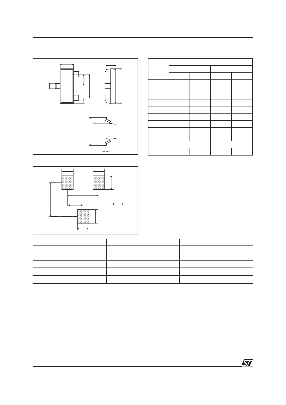
PACKAGE MECHANICAL DATA
SOT23 (Plastic)
E
e
B
FOOTPRINT DIMENSIONS
0.9
0.035
e1
S
L
H
0.9
0.035
A
REF.
Millimeters Inches
DIMENSIONS
Min. Max. Min. Max.
D
A 0.89 1.4 0.035 0.055
A1 0 0.1 0 0.004
B 0.3 0.51 0.012 0.02
A1
c 0.085 0.18 0.003 0.007
D 2.75 3.04 0.108 0.12
e 0.85 1.05 0.033 0.041
e1 1.7 2.1 0.067 0.083
E 1.2 1.6 0.047 0.063
H 2.1 2.75 0.083 0.108
c
L 0.6typ. 0.024 typ.
S 0.35 0.65 0.014 0.026
1.1
0.043
1.9
2.35
0.92
1.45
0.037
0.075
0.9
0.035
mm
inch
1.1
0.043
Orderingtype Marking Package Weight Base qty Delivery mode
BAR42 D94 SOT-23 0.01g 3000 Tape & reel
BAR43 D95 SOT-23 0.01g 3000 Tape & reel
BAR43S DB1 SOT-23 0.01g 3000 Tape& reel
BAR43C DB2 SOT-23 0.01g 3000 Tape& reel
BAR43S DA5 SOT-23 0.01g 3000 Tape& reel
Epoxymeets UL94,V0
Informationfurnished isbelieved to be accurateand reliable.However,STMicroelectronics assumesno responsibility for the consequences of
use of such informationnor for any infringementof patentsor otherrights of third parties whichmay result from its use. No license isgranted
by implication or otherwise under any patent or patentrights of STMicroelectronics.Specifications mentioned in this publication are subject to
change without notice. This publication supersedes and replaces all information previously supplied.
STMicroelectronicsproducts arenotauthorizedforuse ascriticalcomponents in lifesupport devicesorsystems withoutexpress writtenapproval
of STMicroelectronics.
The ST logo is a registered trademark of STMicroelectronics
1999 STMicroelectronics - Printed in Italy -All rights reserved.
Australia - Brazil - China - Finland - France - Germany - Hong Kong - India - Italy - Japan - Malaysia
Malta - Morocco - Singapore - Spain - Sweden - Switzerland - United Kingdom - U.S.A.
STMicroelectronics GROUP OF COMPANIES
http://www.st.com
4/4
 Loading...