

SGS Thomson Microelectronics AVS1ACP08, AVS12CB Datasheet
®
AUTOMATIC VOLTAGE SWITCH (SMPS < 500W)
CONTROLLER
50/60Hz FULL COMPATIBILITY
■
INTEGRATED VOLTAGE REGULATOR
■
TRIGGERING PULSE TRAIN OF THE TRIAC
■
PARASITIC FILTER
■
LOW POWER CONSUMPTION
■
AVS12
A2
TRIAC
HIGHEFFICIENCYANDSAFETYSWITCHING
■
UNINSULATED PACKAGE : AVS12CB
■
V
DRM
I
T(RMS)
= ± 600 V
: 12A
■
■
DESCRIPTION
The AVS12 kit is an automatic mains selector
(110/220V AC) to be used in SMPS < 500 W. It is
composed of 2 devices :
■
The Controller is optimized for low
consumption and high security triggering of the
triac. When connected to V
, the mode input
SS
activates an additional option. If the main
power drops from 220V to 110V, the triac
control remains locked to the 220V mode and
avoids any high voltage spike when the voltage
is restored to 220V.
When connected to V
, the mode input
DD
desactivates this option.
■
The TRIAC is specially designed for this
application. An optimization between sensitivity
and dynamic parameters of the triac gate highly
reduces the losses of supply resistor and allows
excellent immunity against disturbances.
A1
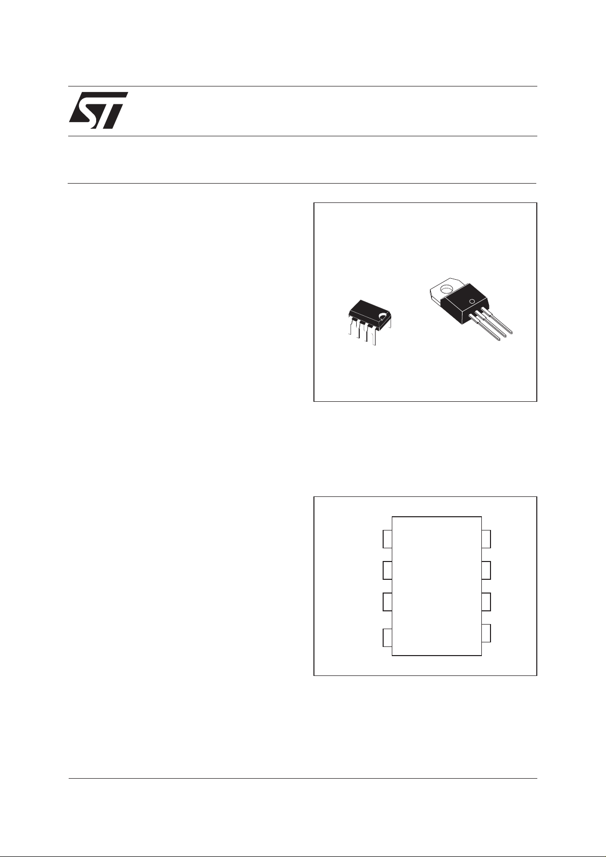
AVS1ACP08
DIP-8
AVS12CB
TO-220AB
PIN CONNECTION
V
SS
Osc / In
Osc / Out N.C.
DD
1
2
3
4
8
7
6
5V
V
Mode
V
A2
G
M
G
January 2002 - Ed: 3C
1/7
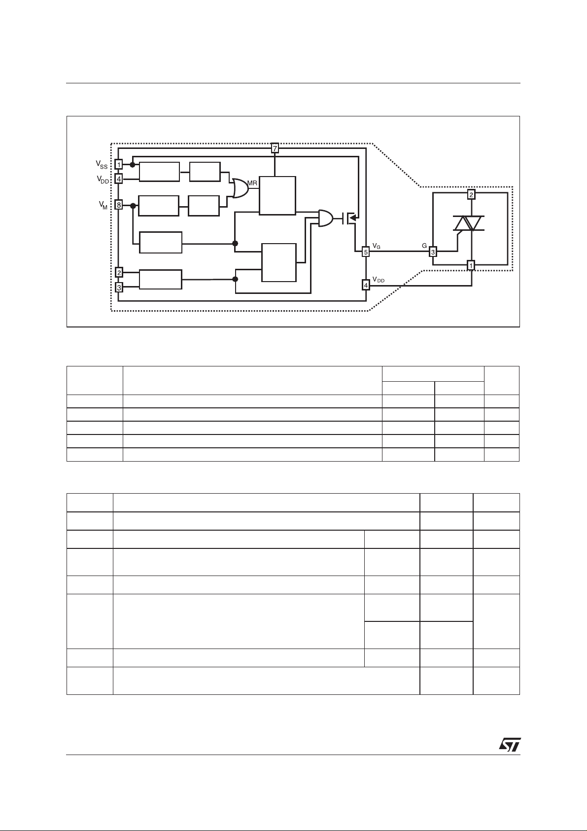
AVS12
BLOCK DIAGRAM
OSC/IN
OSC/OUT
AVS1ACP08
PeakVoltage
Detector
Zero Crossing
Oscillator
Supply
Detector
Reset
Parasitic
Filter
CP
S
CP
MODE
Mains
mode
Controller
Triggering
Time
Controller
AVS12CB
Q
Q
ABSOLUTE MAXIMUM RATINGS
CONTROLLER AVS1ACP08
Symbol Parameter
V
I
V
SS
I/VO
I/IO
Supply voltage -12 0.5 V
I / O voltage VSS-0.5 0.5 V
I / O current -40 +40 mA
Tstg Storage Temperature -60 +150 °C
Toper Operating Temperature code ''C'' 0 +70 °C
Value
Min. Max.
A2
A1
Unit
TRIAC AVS12CB Tj= +25°C (unless otherwise specified)
Symbol Parameter Value Unit
V
DRM
I
T(RMS)
I
TSM
2
I
dI / dt Critical rate of rise of on-state current (1) Repetitive
dV/dt * Linear slope up to 0.67 V
T
stg
T
(1) Gate supply : IG= 100mA – di/dt= 1A/µs *For either polarity of electrode A2 voltage with reference to electrode A1
(2) T
= 110°C
j
2/7
Repetitive peak off-state voltage (2) ± 600 V
RMS on-state current (360° conduction angle) TC= 70°C 12 A
Non repetitive surge peak on-state current ( Tjinitial = 25°C ) t = 8.3ms
t = 10ms
tI
2
t value t = 10ms 50 A2s
F = 50Hz
Non
Repetitive
Gate open Tj = 110°C 50 V/µs
- 40 + 150
0 + 125
Storage Temperature
Junction Temperature Range
j
DRM
105
100
20 A/µs
100
A
°C
AVS12
THERMAL RESISTANCE
TRIAC AVS12CB
Symbol Parameter Value Unit
Rth (j-a) Junction to ambient 60 °C/W
Rth (j-c) DC Junction to case for DC 3 °C/W
Rth (j-c) AC Junction to case for 360° conduction angle (F = 50Hz) 2.3 °C/W
DC GENERAL ELECTRICAL CHARACTERISTICS
TRIAC AVS12CB
Symbol Parameter
V
GD
V
TM
I
DRM
* For either polarity of electrode A2voltage with reference to electrode A
VD=V
RL = 3.3kΩ Pulse duration > 20µs Tj= 110°C 0.2 V
DRM
*ITM= 17A tp= 10ms Tj= 25°C 1.75 V
*V
rated Gate open Tj= 25°C 10 µA
DRM
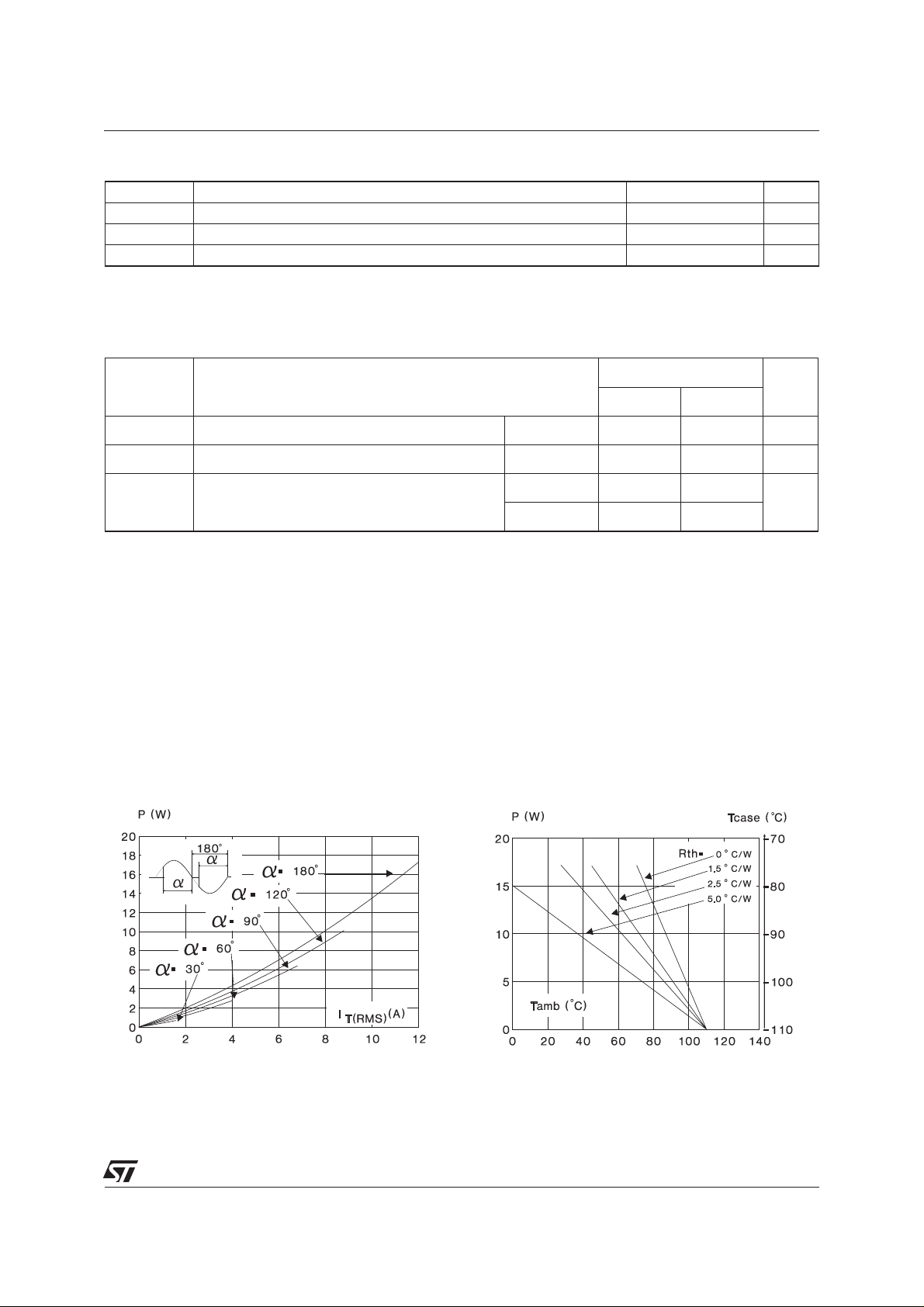
Fig. 1: Maximum RMS power dissipation versus
RMS on-state current (F = 60Hz). (Curves are cut
off by (dI/dt)c limitation)
Value
Unit
Min. Max.
T
= 110°C 500
j
1
Fig. 2: Correlation between maximum mean
power dissipation and maximum allowable temperature (Tamb and Tcase) for different thermal
resistances heatsink + contact.
3/7
 Loading...