

RF & MICROWAVE TRANSISTORS
.REFRACTORY/GOLD METALLIZATION
.EMITTER SITE BALLASTED
.LOW THERMAL RESISTANCE
.INPUT/OUTPUT MATCHING
.OVERLAY GEOMETRY
.METAL/CERAMIC HERMETIC PACKAGE
.P
= 15 W MIN. WITH 5.2 dB GAIN
OUT
AM83135-015
S-BAND RADAR APPLICATIONS
PRELIMINARY DATA
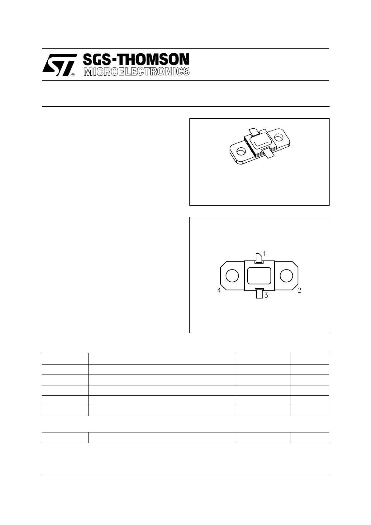
.310 x .310 2LFL (S064)
ORDER CO DE
DESCRIPTION
The AM83135-015 device is a high power silicon
bipolar NPN transistor specifically designed for
S-Band radar pulsed output and driver applications.
This device is characterized at 100µsec pulse
width and 10% duty cycle, but is capable of operation over a range of pulse widths, duty cycles,
and temperatures, and can withstand a 3:1 output VSWR with a + 1 dB input overdrive. Low RF
thermal resistance, refractory/gold metallization,
and computerized automatic wire bonding techniques ensure high reliability and product consistency (including phase characteristics).
The AM83135-015 is supplied in the IMPAC™
Hermetic Metal/Ceramic package with internal
Input/Output impedance matching circuitry, and
is intended for military and other high reliability
applications.
ABSOLUTE MAXIMUM RATINGS (T
Symbol Parameter Value Unit
P
T
DISS
I
V
T
STG
C
CC
J
Power Dissipation* (TC ≤ 50˚C) 71 W
Device Current* 3.0 A
Collector-Supply Voltage* 46 V
Junction Temperature (Pulsed RF Operation) 250
Storage Temperature
case
= 25°C)
AM83131-015
PIN CONNECTION
1. Collector 3. Emitter
2. Base 4. Base
65 to +200
−
BRANDING
83135-15
°
C
°
C
THERMAL DATA
R
TH(j-c)
*Applies only to rated RF amplifier operation
July 27, 1994
Junction-Case Thermal Resistance* 2.8
°
C/W
1/3

AM83135-015
ELECTRICAL SPECIFICATIONS (T
case
= 25°C)
STATIC
Symbol Test Condi tions
BV
CBOIC
BV
EBOIE
BV
CERIC
I
CES
h
FE
= 10 mA IE = 0 mA 55 — — V
= 2 mA IC = 0 mA 3.5 — — V
= 10 mA RBE = 10 Ω 55 — — V
VBE = 0 V VCE = 40 V — — 8 mA
VCE = 5 V IC = 1 A 30 — 300 —
DYNAMIC
Symbol Test Conditi ons
P
OUT
η
P
Note: Pulse Widt h
f = 3.1 − 3.5 GHz PIN = 4.5 W VCC = 40 V 15 — — W
cf = 3.1 − 3.5 GHz P
f = 3.1 − 3.5 GHz P
G
100µS
=
Duty Cycle=10%
= 15 W VCC = 40 V 30 — — %
OUT
= 15 W VCC = 40 V 5.2 — — dB
OUT
Valu e
Min. Typ. Max.
Value
Min. Typ. Max.
Unit
Unit
2/3
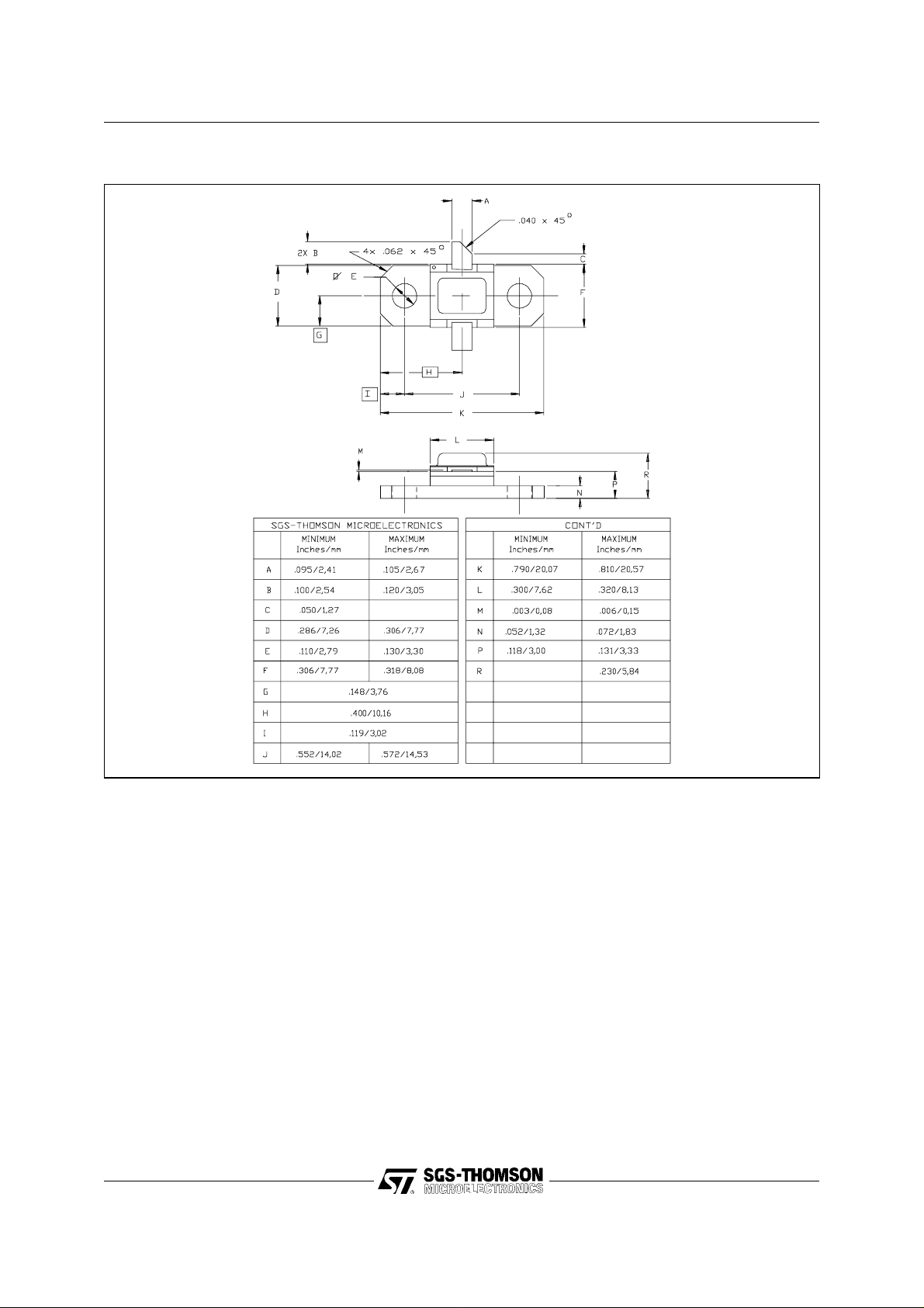
PACKAGE MECHANICAL DATA
Ref.: Dwg. No. 12-0221 rev. A
AM83135-015
Information furnished is believed to be accurate and reliable. However, SGS-THOMSON Microelectronics assumes no responsibility
for the cons equences of us e of such inform ation nor for any infri ngement of patents or other rights of third par ties which may re sul t
from its use. No lice nse is gr anted by impl icati on or otherw ise under any pate nt or patent rights of SGS-TH OMSON Mic roelect ronics.
Specifications mentioned in this publication are subject to change without notice. This publication supersedes and replaces all
informati on previo usly suppl ied. SGS-TH OMSON Microe lectronics products are not author ized for us e as critical c omponents in life
support devices or systems without express written approval of SG S-TH OMS ON Mic roelec t roni cs.
© 1994 SGS -TH OMSO N M icro elec tron ic s - All Ri ghts Rese rve d
Australia - Braz il - F rance - Ger man y - H ong Kon g - Ital y - Jap an - K orea - Ma lays ia - Malt a - Mor occ o - T he Nether lan ds -
Singapore - Spain - Sweden - Swit zerland - Taiwan - Thaila nd - United Kingd om - U.S.A.
SGS-THOMSON Microele ctronics GROUP OF C OMPANIES
3/3
 Loading...