

RF & MICROWA VE TRANSIST ORS
.REFRACTORY/GOLD METALLIZATION
.EMITTER SITE BALLASTED
.LOW THERMAL RESISTANCE
.INPUT/OUTPUT MATCHING
.OVERLAY GEOMETRY
.METAL/CERAMIC HERMETIC PACKAGE
.P
OUT
DESC RIPT ION
The AM81719-030 is a high power silicon NPN
bipolar transistor designed for Class C, CW communications and telemetry applications in the 1.75
- 1.85 GHz frequency range.
An emitter site ballasted refractory/gold overlay
die geometry computerized automatic wirebonding
is employed to ensure long term reliability and
product consistency.
AM81719-030 is supplied in the industry-standard
AMPAC hermetic metal/ceramic package.
28 W MIN. WITH 6.7 dB GAIN
=
AM81719-030
TELEMETRY APPLICATIONS
PRELIMINARY DATA
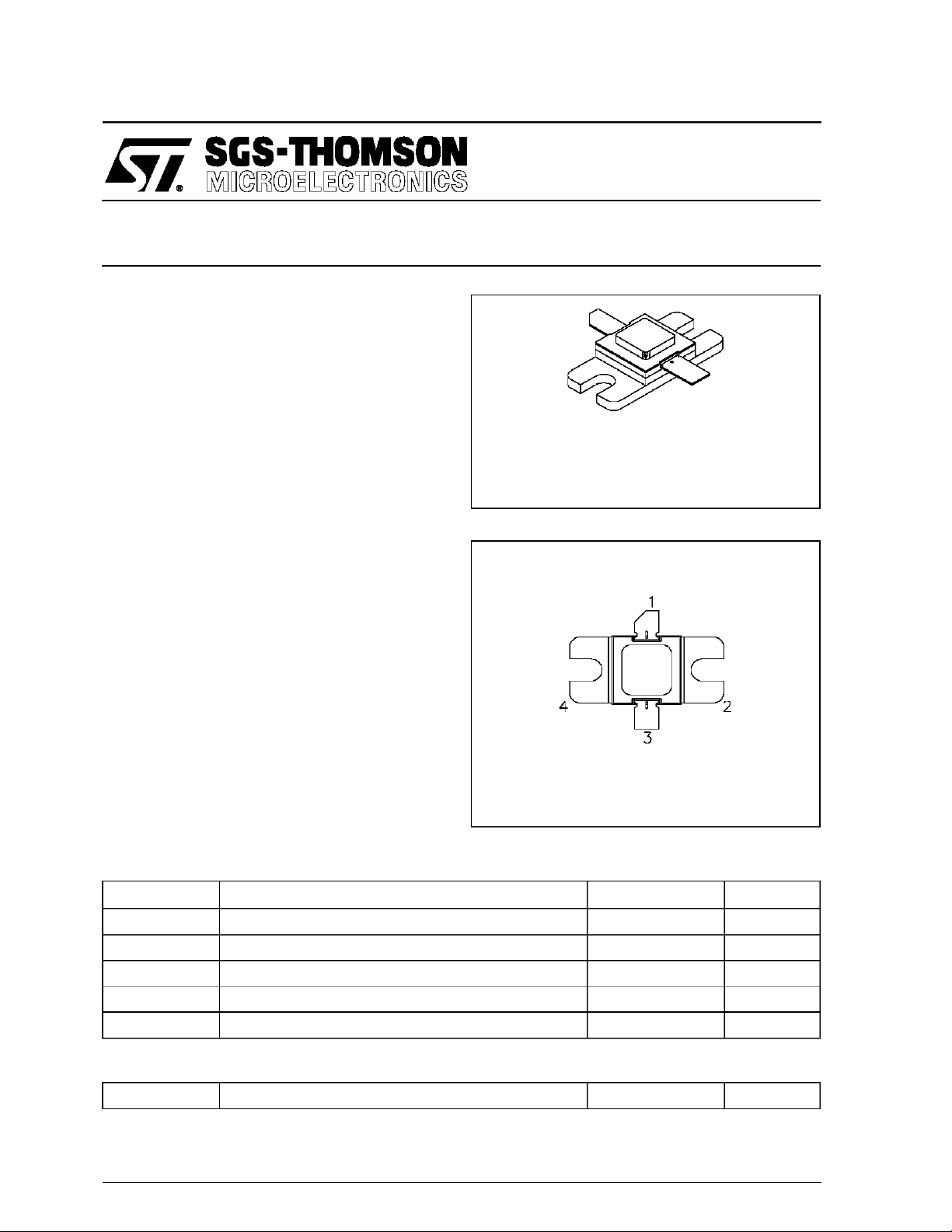
.400 SQ 2LFL (M147)
hermetically sealed
ORDER CODE
AM81719-030
PIN CONNE C TIO N
1. Collector 3. Emitter
2. Base 4. Base
BRAND I NG
81719-030
ABSOLUTE MAXIMUM RATINGS (T
Symbol Parameter Value Uni t
P
DISS
I
C
V
CC
T
J
T
STG
THERMA L DA TA
R
TH(j-c)
*Appliesonly to ratedRF amplifieroperation
September 1992
Power Dissipation* 67.3 W
Device Current* 2.67 A
Collector-Supply Voltage* 28 V
Junction Temperature 200
Storage Temperature − 65 to +200
Junction-Case Thermal Resistance* 2.6 °C/W
case
= 25°C)
°
C
°
C
1/4
AM81719-030
ELECTRICAL SPECIF ICATIO NS (Tcase = 25°C)
STATIC
Symbol Test Conditions
BV
BV
BV
I
CES
h
CBO
EBO
CES
FE
IC= 10mA IE= 0mA 45 — — V
IE= 10mA IC= 0mA 3.0 — — V
IC = 10mA 45 — — V
VBE= 0V VCE= 28V — — 5 mA
VCE= 5V IC= 2mA 15 — 150 —
Min. Typ. Max.
DYNAMIC
Symbol Test Conditi ons
P
OUT
η
cf=1.75 — 1.85GHz PIN= 6.0W VCC= 28V 40 — — %
G
P
f = 1.75 — 1.85GHz PIN= 6.0W VCC= 28V 28 — — W
f = 1.75 — 1.85GHz PIN= 6.0W VCC= 28V 6.7 — — dB
Min. Typ. Max.
Value
Value
Unit
Unit
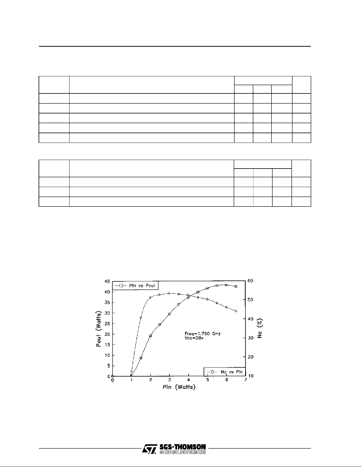
TYPICA L PERFO R MA NCE
POWER OUTPUT & CO LLECTOR
EFFICENCY vs POWER INPUT
2/4
 Loading...