RF & MICROWAVE TRANSISTORS
SPECIA LITY AVIONIC S/JTI DS APPLICAT IONS
.REFRACTORY/GOLD METALLIZATION
.EMITTER SITE BALLASTED
. 15: 1 VSWR CAPABILITY
. LOW RF THERMAL RESISTANCE
.INPUT/OUTPUT MATCHING
.O VERLAY GEOMETRY
.METAL/CERAMIC HERMETIC PACKAGE
.P
OUT
30 W MIN. WITH 7.8 dB GAIN
=
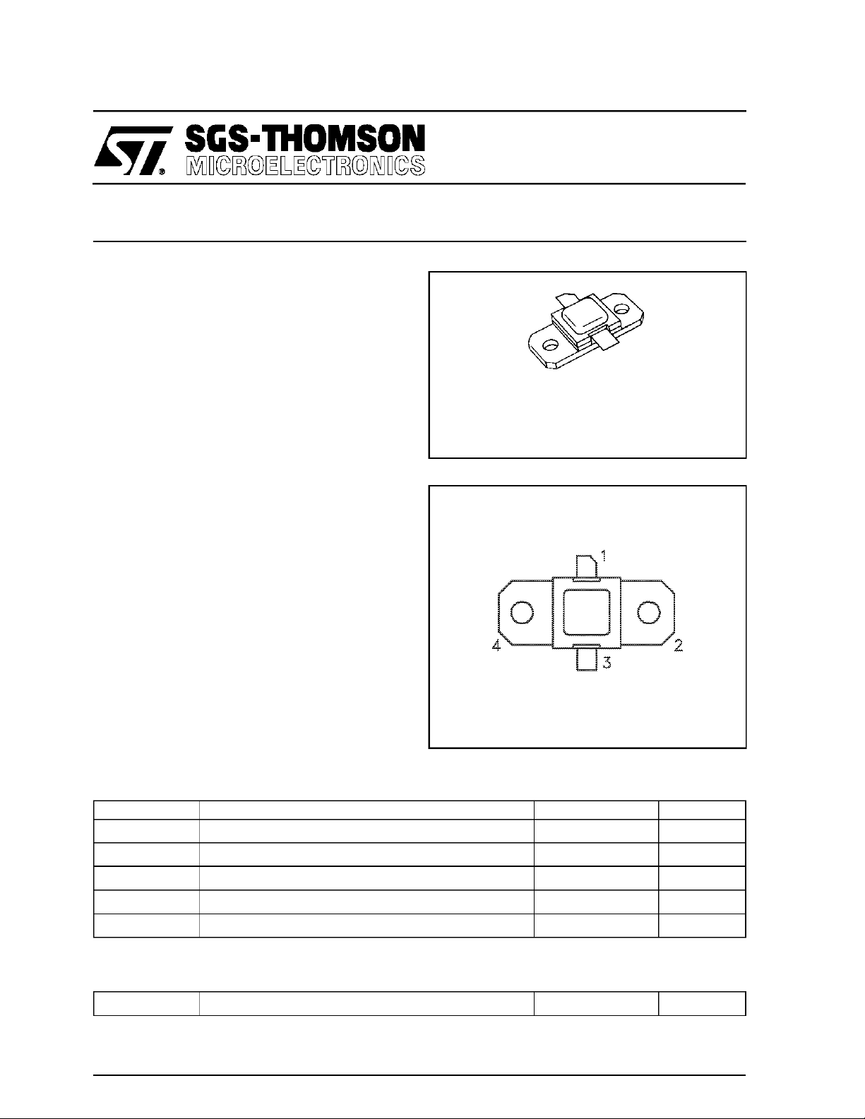
.400 x .400 2LFL (S036)
hermetically sealed
ORDER CODE
AM80912-030
AM80912-030
BRAND I NG
80912-30
DESCRIPT I ON
The AM80912-030 device is a high power Class C
transistorspecifically designedforJTIDS pulsedoutput anddriverapplications.
Thisdeviceis capable ofoperation over a widerange
of pulse widths, duty cycles and temperatures and is
capable of withstanding 15:1 output VSWR at rated
RF conditions.
Low RF thermal resistance and computerized automaticwirebonding techniques ensure high reliability
and product consistency.
The AM80912-030 is supplied in the hermetic metal/ceramic package with internal input matching
structures.
ABSOLU TE MAXI MUM RATING S (T
Symbol Parameter Value Uni t
P
T
DISS
I
V
CC
T
STG
C
J
Power Dissipation* (TC≤ 85°C) 75 W
Collector Current* 3.5 A
Collector-Supply Voltage* 40 V
Junction Temperature (Pulsed RF Operation) 250
Storage Temperature − 65 to +200
case
= 25°C)
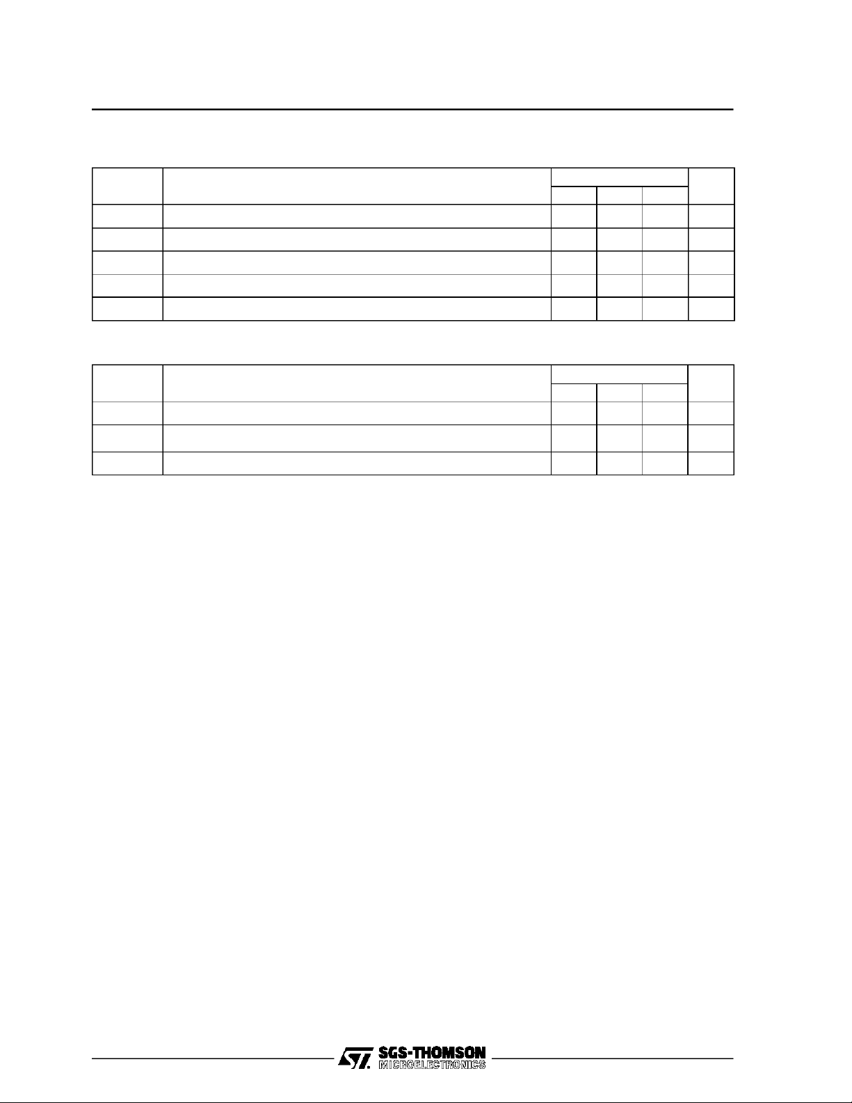
PIN CONNECTION
1. Collector 3. Emitter
2. Base 4. Base
°
C
°
C
THERMA L DAT A
R
TH(j-c)
*Appliesonly to rated RFamplifieroperation.
August 1992
Junction-Case Thermal Resistance 2.2 °C/W
1/6

AM80912-030
ELEC TRICAL SPECIF ICA TIONS (T
case
25° C)
=
STATIC
Symbol Test Condition s
BV
BV
BV
I
CES
h
CBO
EBO
CER
FE
IC= 10mA 55 — — V
I
1mA 3.5 — — V
=
E
I
20mA R
=
C
V
35V — — 5.0 mA
=
CE
V
5V I
=
CE
10Ω 55 — — V
=
BE
1.0A 15 — 150 —
=
C
DYNAMIC
Symbol Test Condition s
P
OUT
η
C
G
P
Note: Pulse fo rmat: 6.4 µson6.6µs off, repeat f or 3. 3 ms, then of f for 4.5125 ms.
f=960 — 1215MHz P
f = 960 — 1215MHz P
f=960 — 1215MHz P
Duty Cycle: Burst 49.2%, over all 20.8%
IN
IN
IN =
5.0W V
=
5.0W V
=
5.0W V
+35V 30 36 — W
=
CC
+35V 40 45 — %
=
CC
+35V 7.8 8.6 — dB
CC =
Value
Min. Typ. Max.
Value
Min. Typ . Max.
Unit
Unit
2/6
 Loading...