

RF & MICROWAVE TRANSISTORS
S-BAND RADAR APPLICA TIONS
.REFRACTORY/GOLD METALLIZATION
.EMITTER SITE BALLASTED
. 3: 1 VSWR CAPABILITY
. LOW THERMAL RESISTANCE
.INPUT/OUTPUT MATCHING
.O VERLAY GEOMETRY
.METAL/CERAMIC HERMETIC PACKAGE
.P
105 W MIN. WITH 6.2 dB GAIN
OUT =
.400 x . 500 2L SF L (S 138)
ORDER CODE
AM2931-110
AM2931-110
hermetically sealed
BRANDING
2931-110
DESC RIPT ION
The AM2931-110 is a high power silicon bipolar
NPN transistor specifically designed for S-Band
radar pulsed output and driver applications.
This device is capable of operation over a wide
range of pulse widths, duty cycles and temperatures and can withstand a 3:1 output VSWR. Low
RF thermal resistance, refractory/gold metallization, and computerized automatic wire bonding
techniques ensure high reliability and product consistency (including phase characteristics).
The AM2931-110 is supplied in the BIGPAC Hermetic Metal/ Cerami c package with i nternal
Input/Output matching circuitry, and is intended
for military and other high reliability applications.
ABSOLU TE M AXI MUM RATING S (T
Symbol Parameter Value Uni t
P
T
DISS
I
V
CC
T
STG
C
J
Power Dissipation* (TC≤ 100°C) 375 W
Device Current* 12 A
Collector-Supply Voltage* 48 V
Junction Temperature (Pulsed RF Operation) 250
Storage Temperature − 65 to +200
case
= 25°C)
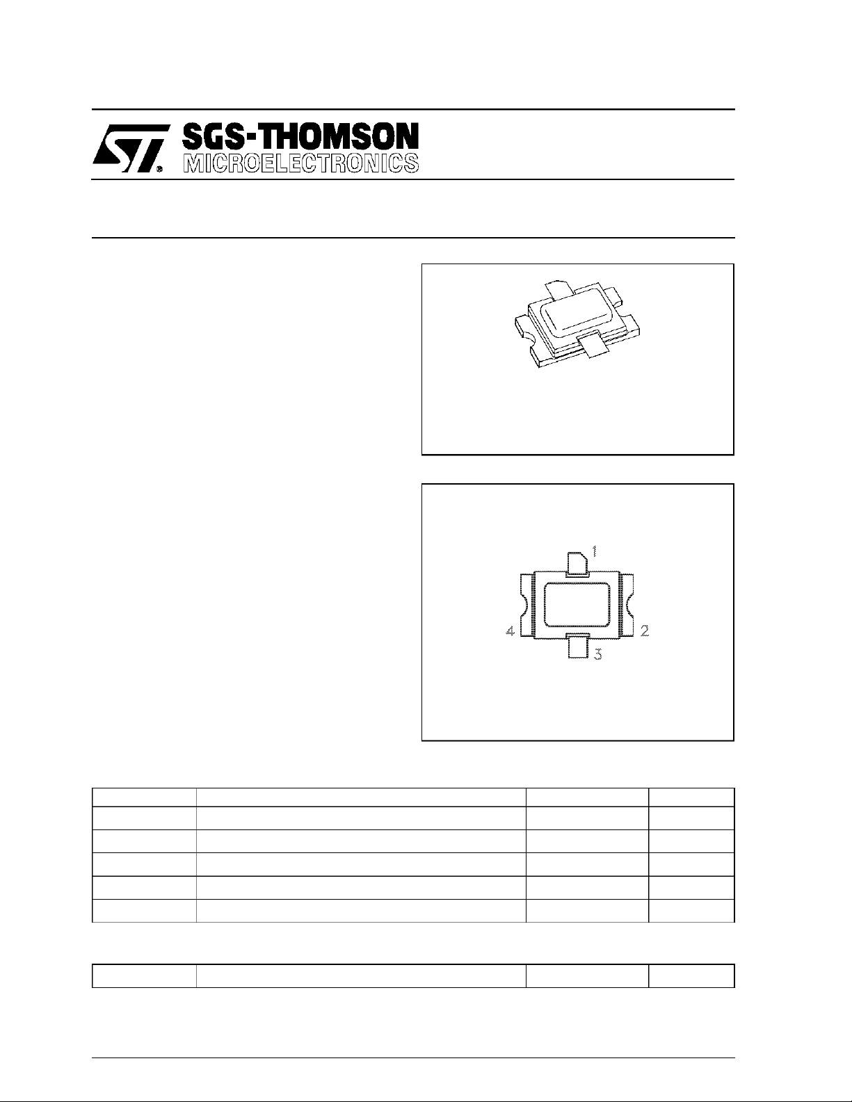
PIN CO NNE C TIO N
1. Collector 3. Emitter
2. Base 4. Base
°
C
°
C
THERMA L DATA
R
TH(j-c)
*Appliesonly torated RFamplifieroperation
August 1992
Junction-Case Thermal Resistance* 0.40 °C/W
1/4

AM2931-110
ELEC TRICAL SPEC I F ICA TIONS (Tcase = 25°C)
STATIC
Symbol Test Condition s
BV
CBO
BV
EBO
BV
CER
I
CES
h
FE
DYNAMIC
Symb ol Test Co n dit i o ns
P
OUT
η
cf=2900 — 3100MHz P
G
P
Note: Pulse Width
IC= 40mA IE= 0mA 55 — — V
IE= 8mA IC= 0mA 3.5 — — V
IC = 40mA RBE= 10Ω 55 — — V
VBE= 0V VCE= 42V — — 30 mA
VCE= 5V IC= 4A 30 — — —
f = 2900 — 3100MHz P
f = 2900 — 3100MHz P
50 µSec
=
Duty Cycle=10%
25W V
=
IN
25W V
=
IN
25W V
=
IN
Value
Min. Typ. M ax.
Value
Min. Typ. Max.
42V 105 115 — W
=
CC
42V 32 40 — %
=
CC
42V 6.2 6.6 — dB
=
CC
Unit
Uni t
TYPICAL PERFORM AN CE
TYPICAL BROADBAND
PERFORMANCE
PIN(W)
28
24
20
VCC- 42 Volts
PW - 50 µSec
DC - 10%
TC-25°C
PIN(W)
20
24
28
2/4

IMPEDA NCE DATA
TYPICAL INPUT
IMPEDANCE
Z
IN
TYPICAL COLLECTOR
LOAD IMPEDANCE
AM2931-110
Z
CL
FREQ. ZIN(Ω)Z
L = 2.9 GHz 15.0 − j 9.0 5.0 − j 1.0
M = 3.0 GHz 20.0 − j 9.5 4.8 + j 0.5
H = 3.1 GHz 13.5 − j 5.0 3.5 + j 2.5
TEST CIRCUIT
CL
(Ω)
PIN= 25 W
VCC= 42 V
Normalized to 50 ohms
All dimensions are in inches.
Substrate material: .025 thick AI2O3(Er=9.6)
C1 : 1500 pF RF Feedthrough
C2 : 1 µF, CK06 CapacitorC
C3 : 1 µF, Tantalum Capacitor
C4 : 100 µF Electrolytic Capacitor, 63V
C5 : 22 pF Chip Capacitor (bridge at location indicated)
RFC1 : Gold Plated Nickel Strap, 0.060 Inch Wide,
RFC2 : No. 26 Wire, 2 Turn .0.80 Inch I.D.
0.005 Inch Thick, 0.290 Inch Long
3/4

AM2931-110
PACKAGE MECHANICAL DATA
Information furnished is believed tobe accurate and reliable.However, SGS-THOMSON Microelectronics assumes no responsability for the
consequences of useof such information norfor any infringement ofpatents or other rights of thirdpartieswhich may results from itsuse. No
license isgranted byimplication or otherwiseunderany patent orpatent rights ofSGS-THOMSON Microelectronics.Specificationsmentioned
in this publicationaresubject to change without notice.This publication supersedes andreplaces all information previously supplied.
SGS-THOMSON Microelectronicsproducts arenotauthorized foruse ascritical componentsin lifesupport devicesorsystems withoutexpress
written approvalof SGS-THOMSON Microelectonics.
1994 SGS-THOMSON Microelectronics- All Rights Reserved
Australia - Brazil - France- Germany - Hong Kong - Italy-Japan - Korea - Malaysia -Malta - Morocco -The Netherlands -
Singapore -Spain- Sweden- Switzerland -Taiwan - Thailand- UnitedKingdom - U.S.A
SGS-THOMSON MicroelectronicsGROUP OF COMPANIES
4/4
 Loading...