

ADB18PS
February 1998 - Ed: 2
Peakpulse powerdissipation100W (8/20µs)
Stand-offvoltage:18 V
MaximumDCcurrent: 0.5 A
Clampingvoltage:V
CL
< 50 V (8/20 µs)
FEATURES
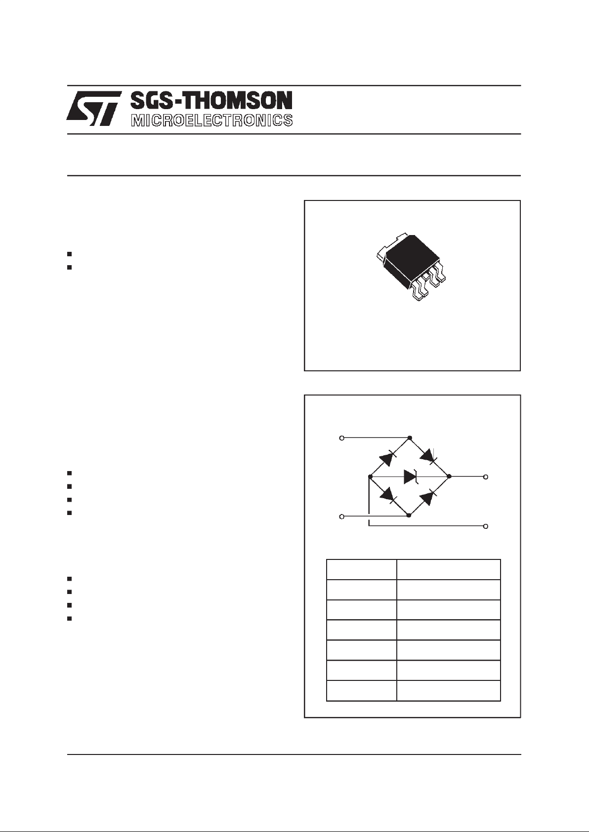
PPAK-5L
1
TAB
2
3
4
5
PIN-OUTCONFIGURATION
1
5
2
4
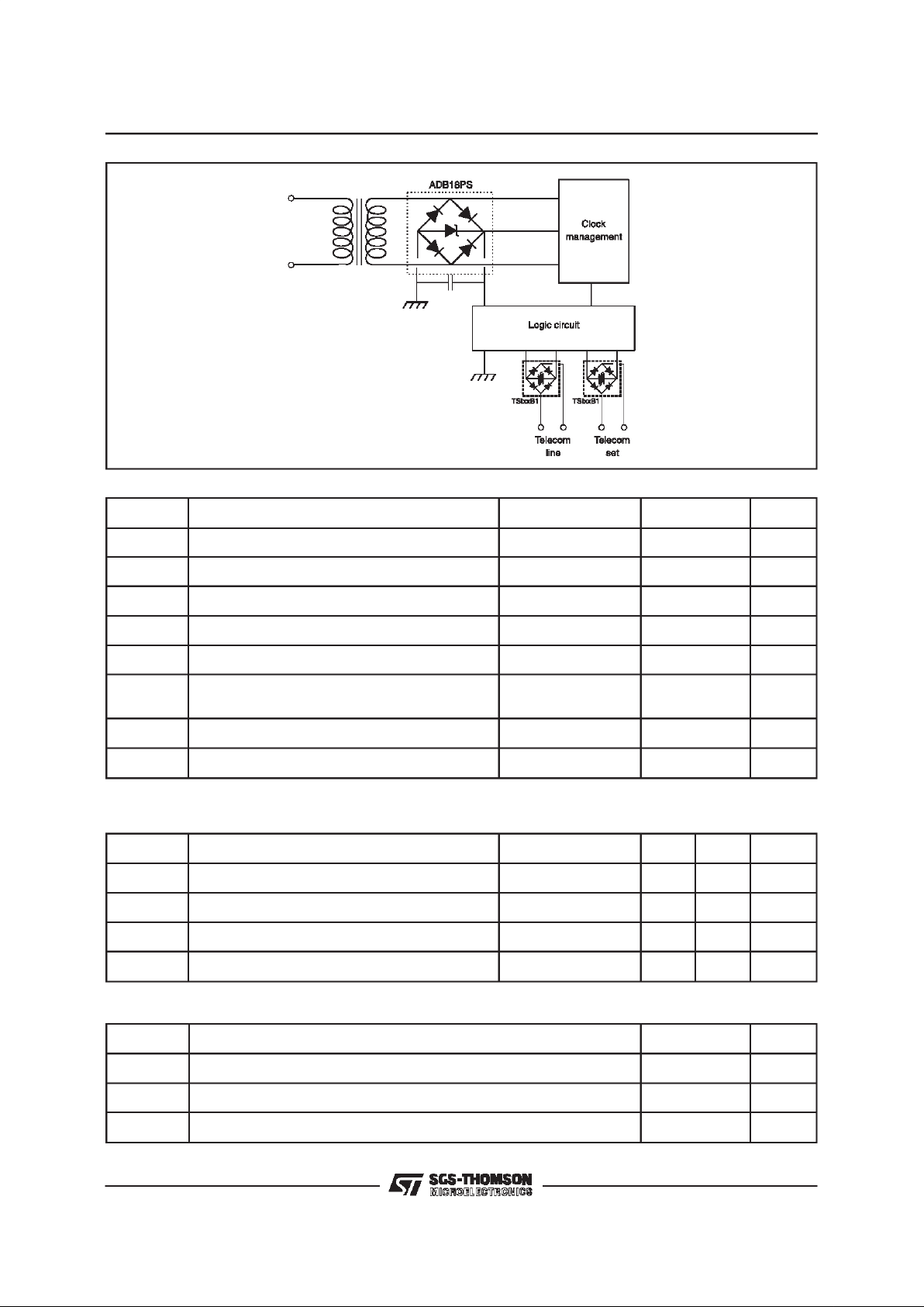
Protectioncombinedwith rectification
Highreliabilityconferedby monolithicconstruction
Spacesaving
Costeffective solution
BENEFITS
AUTOPROTECTED
DIODE BRIDGE
Application Specific Discretes
A.S.D.
TM
Any electronic equipment needing a diode bridge
andprotection against transientovervoltage:
CallerId
Handset
MAINAPPLICATIONS
The ADB18PS combines a diode bridge and a
clampingprotection function.
Integrated monolithically within a SMD package,
this device allows space saving and greater
reliability.
It provides both rectificationand protectionfor low
powerequipment directlysuppliedby mains.
DESCRIPTION
Pin Description
1 DC output
2 AC input
3 Notaccessible
4 AC input
5 DC output
TAB Not to be connected
1/3
Symbol Parameter Testconditions Value Unit
P
PP
Peak pulsepowerdissipation(one pulse) 8 /20 µs 100 W
P Powerdissipation T
case
=70°C20W
V
RRM
Repetitivepeak reversevoltage 18 V
I
PP
Peak pulsereversecurrent (one pulse) 8 / 20µs2A
I
F
Forwardcurrent for onediode 0.5 A
I
FSM
Non repetitivesurge peakforward current tp= 8.3ms
t
p
=10ms
8
7.5
A
T
stg
Storagetemperaturerange -40 to 150 °C
T
j
Maximumjunction temperature 150 °C
ABSOLUTE MAXIMUM RATINGS
(T
amb
=25°C, unless otherwise specified)
APPLICATIONCIRCUIT : Caller Id interface
Symbol Parameter Testconditions Typ Max Unit
V
CL
Clampingvoltage IPP=2 A 8/20µs50V
I
RM
Leakagecurrent VRM=18V 2
µ
A
V
F
Forwardvoltage for one diode IF= 500mA 1.4 V
C Capacitance
V
R
=0V,F=1MHz
50 pF
ELECTRICALCHARACTERISTICS (T
amb
=25°C).
Symbol Parameter Value Unit
R
th(j-a)
Junctionto ambienton FR4 (0.5 cm2)
80 °C/W
R
th(j-a)
Junctionto ambienton IMS (17 cm2)30°C/W
R
th(j-c)
Junctionto case
4 °C/W
THERMAL RESISTANCES
ADB18PS
2/3

PACKAGEMECHANICAL DATA
PPAK-5L
Information furnished isbelieved to be accurate and reliable. However, SGS-THOMSON Microelectronics assumes no responsibility for the
consequences of use of such information nor for any infringement of patents or other rights of third partieswhich may result from its use. No
license is grantedby implication or otherwise under any patent or patent rights of SGS-THOMSON Microelectronics. Specificationsmentioned
in this publication are subject tochange withoutnotice. This publicationsupersedes and replacesall informationpreviously supplied.
SGS-THOMSONMicroelectronics products arenot authorizedfor useas critical components in life support devices or systems without express
written approval of SGS-THOMSON Microelectronics.
1998 SGS-THOMSON Microelectronics- Printed in Italy -All rights reserved.
SGS-THOMSON Microelectronics GROUP OF COMPANIES
Australia - Brazil - Canada - China - France - Germany - Italy - Japan - Korea - Malaysia - Malta - Morocco
The Netherlands - Singapore- Spain - Sweden- Switzerland - Taiwan - Thailand - UnitedKingdom - U.S.A.
REF.
DIMENSIONS
Millimeters Inches
Min. Typ. Max Min. Typ. Max.
A 2.20 2.40 0.0866 0.0945
A1 0.90 1.10 0.0354 0.0433
A2 0.03 0.23 0.0001 0.0009
B 0.4 0.90 0.0157 0.0236
B2 5.20 5.40 0.2047 0.2126
C 0.45 0.60 0.0177 0.0236
C2 0.48 0.60 0.0188 0.0236
D 6.00 6.20 0.2362 0.2441
E 6.40 6.60 0.2519 0.2598
G 4.9 5.25 0.1929 0.2067
G1 2.38 2.7 0.0937 0.1063
H 9.35 10.10 0.369 0.3977
L2 0.80 1.00 0.0314 0.0393
L4 0.60 1.00 0.0236 0.0393
R 0.2 0.0078
V2 0° 8° 0° 8°
Package Type Marking
PPAK-5L ADB18PS ADB18
MARKING
ORDERCODE
ADB 18 PS RL
Reversevoltage
PPAK-5L
PACKAGING:
RL= tape& reel(baseqty=2500pcs)
=tube(baseqty = 75pcs)
ADB18PS
3/3
 Loading...