

®
ACST8-8C
ASD™
AC Switch Family
MAIN APPLICATIONS
AC static switching in appliance & industrial
■
control systems
Washing machine with bi-rotational induction
■
motor drive
Induction motor drive for:
■
- refrigerator / freezer compressor
- air conditioning compressor
FEATURES
V
■
DRM/VRRM
Avalanche controlled device
■
■ I
T(RMS)
High noise immunity: static dV/dt > 750 V/µs
■
Gate triggering current : IGT<30mA
■
■ Snubberless turn off commutation:
(dI/dt)c > 4.5A/ms
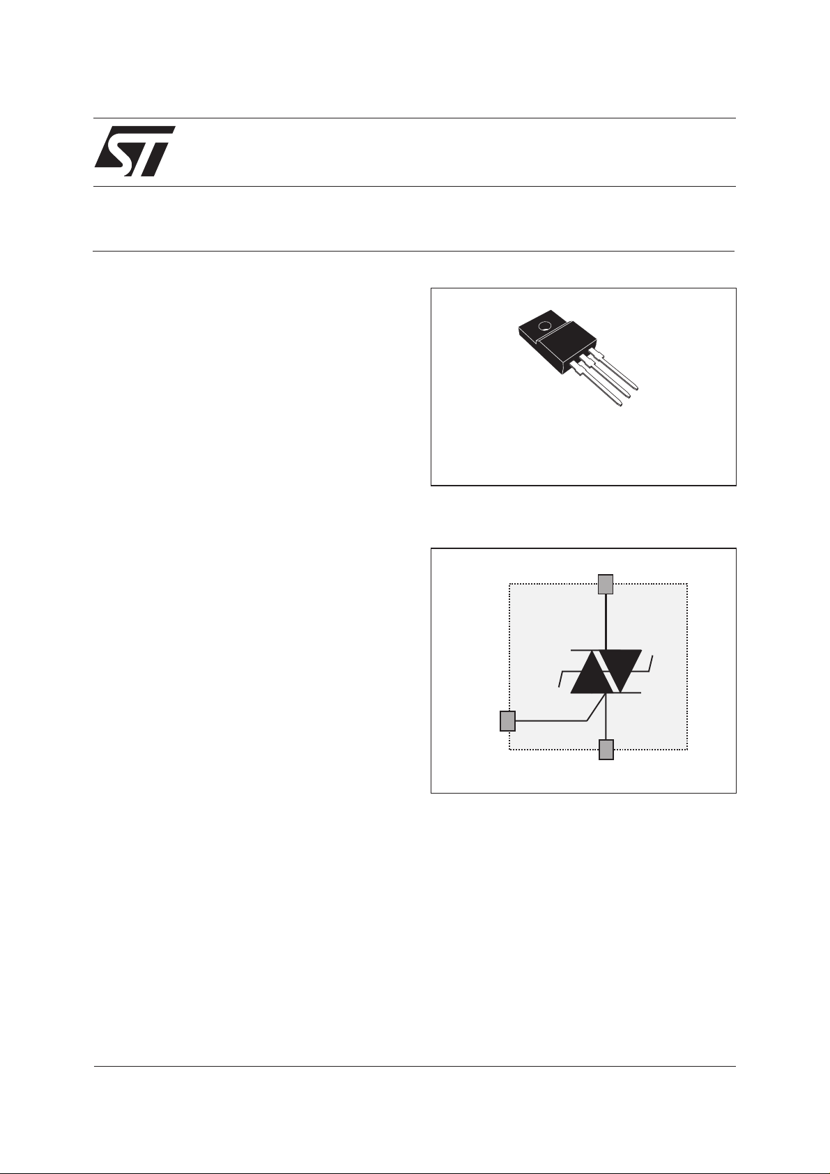
■ TO-220FPAB package
= +/- 800V
= 8A with T
CASE
=90°C
OVER VOLTAGE PROTECTED
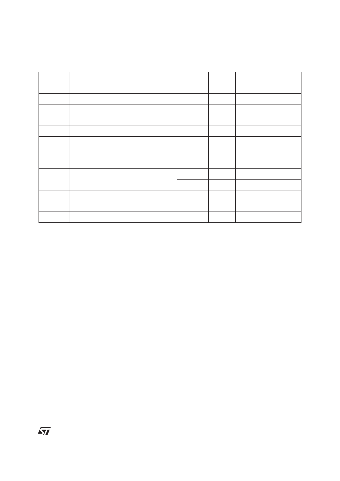
AC POWER SWITCH
G
OUT
COM
TO-220FPAB
FUNCTIONAL DIAGRAM:
OUT
BENEFITS
■
Enables equipment to meet EN61000-4-5
standard
■
High off-state reliability with planar technology
■
Need no external overvoltage protection
■
Reduces the power component count
DESCRIPTION
The ACST8-8C belongs to the AC power switch
family built around the ASD technology. This high
performance device is adapted to home appliances
or industrial systems and drives an induction motor
up to 8A.
This ACST switch embeds a triac structure with a
high voltage clamping device to absorb the inductive
turn off energy and withstand line transients such as
those described in the IEC61000-4-5 standards.
G
COM
January 2002 - Ed: 4B
1/8

ACST8-8C
ABSOLUTE RATINGS (limiting values)
Symbol Parameter Value Unit
V
DRM /
V
RRM
I
T(RMS)
I
TSM
2
I
t Thermal constraint for fuse selection tp = 10ms 35 A2s
dI/dt Non repetitive on-state current critical rate of rise
V
PP
Tstg Storage temperature range - 40 to + 150 °C
Tj Operating junction temperature range - 40 to + 125 °C
Tl Maximum lead soldering temperature during 10s 260 °C
Note 1:accordingto test described by IEC61000-4-5 standard & Figure A.
GATE CHARACTERISTICS (maximum values)
Symbol Parameter Value Unit
P
G (AV)
P
GM
I
GM
Repetitive peak off-state voltage 800 V
RMS on-state current full cycle sine wave 50 to 60 Hz Tcase = 90°C 8 A
Non repetitive surge peak on-state current
Tj initial = 25°C, full cycle sine wave
tp = 20ms 80 A
tp = 16.7ms 85 A
Rate period > 1mn 100 A/µs
I
= 10mA (tr < 100ns)
G
Non repetitive line peak pulse voltage
note 1
2kV
Average gate power dissipation 0.1 W
Peak gate power dissipation (tp = 20µs) 10 W
Peak gate current (tp = 20µs) 1 A
THERMAL RESISTANCE
Symbol Parameter Value Unit
Rth (j-a) Junction to ambient 60 °C/W
Rth (j-c) Junction to case for full cycle sine wave conduction 3.5 °C/W
PARAMETER DESCRIPTION
Parameter Symbol Parameter description
I
GT
V
GT
V
GD
I
H
I
L
V
TM
V
TO
R
D
I
DRM/IRRM
dV/dt Static pin OUT voltage rise
Gate triggering current
Gate triggering voltage
Non triggering voltage
Holding current
Latching current
On state voltage
On state characteristic threshold voltage
On state characteristic dynamic resistance
Forward or reverse leakage current
(dI/dt)c Turn off current rate of decay
V
CL
Avalanche voltage at turn off
2/8
ACST8-8C
ELECTRICAL CHARACTERISTICS PER SWITCH
For either positive or negative polary of pin OUT voltage respect to pin COM voltage
Symbol Test conditions Values Unit
I
V
V
V
V
R
I
DRM
I
RRM
GT
GT
GD
I
H
I
L
TM
TO
D
V
= 12V (DC) RL=33Ω Tj = 25°C MAX. 30 mA
OUT
V
= 12V (DC) RL=33Ω Tj = 25°C MAX. 1.5 V
OUT
V
OUT=VDRM
I
= 100mA Gate open Tj = 25°C MAX. 40 mA
OUT
RL= 3.3kΩ Tj =125°C MIN. 0.2 V
IG= 20mA Tj = 25°C MAX. 70 mA
I
= 11A tp = 380µs Tj = 25°C MAX. 1.5 V
OUT
Tj = 125°C MAX. 0.95 V
Tj = 125°C MAX. 50 mΩ
V
OUT=VDRM
V
OUT=VRRM
Tj = 25°C MAX. 10 µA
Tj = 125°C MAX. 1 mA
dV/dt V
= 550V gate open Tj = 125°C MIN. 750 V/µs
OUT
(dI/dt)c Withoutsnubber Tj = 125°C MIN. 4.5 A/ms
V
CL
ICL= 1mA tp = 1ms Tj = 25°C TYP. 1200 V
AC LINE SWITCH BASIC APPLICATION
The ACST8-8C device is especially designed to drive medium power induction motors in washing machines, refrigerators, dish washers, and tumble dryers.
Pin COM : Common drive reference, to be connected to the power line neutral
Pin G :Switch Gate input to be connected to the controller
Pin OUT : Switch Output to be connected to the load
When driven from a low voltage controller, the ACST switch is triggered with a negative gate current flowing out of the gate pin G. It can be driven by the controller through a resistor as shown on the typical application diagram. In appliance systems, the ACST8-8C switch intends to drive medium power load in ON /
OFF full cycle or phase angle control mode.
Thanks to its thermal and turn-off commutation characteristics, the ACST8-8C switch is able to drive
an inductive load up to 8A without a turn-off aid snubber circuit.
In washing machine or drier appliances, the tumble rotates in both directions. When using bidirectional
phase shift induction motor, two switches are connected on each side of the phase shift capacitor: in
steady-state operation, one switch only conducts energising the coils and defining the tumble direction.
3/8

ACST8-8C
TYPICAL APPLICATION DIAGRAM
OUT
G
COM
CONTROL
UNIT
ROBUSTNESS AGAINST FAST CAPACITOR DISCHARGE
When parasitic transients or controller mis-operation occur, the blocked switch may turn on by spurious
switch firing. Since the phase shift capacitor is charged, its energy is instantaneously dissipated through
the two ACSTs whichcanbedestroyed.Topreventsuchafailure,aresistiveinductivecircuit R-L is added
in series with the phase shift capacitor.
The dI/dt depends on the maximal voltage V
tions), and on the inductance L:
dIdtV
max
=
L
The total switch turn on di/dt isthe sum of the di/dt created by any RC noise suppressor discharge and the
dI/dt created by the motor capacitor discharge.
Sincethemaximaldi/dtcapability at turn-on of the ACST8 is 100A/µs,themotorcapacitor di/dt is assumed
to be less than 50A/µs; therefore, the inductance should be 14µH.
The resistor R limits the surge current through the ACST8 during the capacitor discharge according to the
specifiedcurveI
=f(tp)asshown in Figure 6
TSM
dissipation (usually less than 1 W).
Finally both the 14µH inductance and the 1.2Ω resistance provide a safety margin of two onthe surge cur-
rent I
described in Figure 6.
TSM
of the phase shift capacitor (700V on 240V mainsapplica-
max
(tobeissued)
,and1.2Ωis low enough to limit the resistor
4/8
M
V
AC
C
L
R
Fast capacitor discharge when
one ACST switch turns on (T2)
and the motor runs (T1 ON).
700V
T1
ON
T2

ACST8-8C
AC LINE TRANSIENT VOLTAGE RUGGEDNESS
The ACST8-8C switch is able to safely withstand the AC line transient voltages either by clamping the low
energy spikes or by breaking over under high energy shocks.
The test circuit in Figure A is representative of the ACST application and is used to test the ACST switch
according to the IEC61000-4-5 standard conditions.Thankstotheloadimpedance,theACSTswitchwithstands voltage spikes up to 2 kV above the peak line voltage by breaking over safely. Such non repetitive
testing can be done 10 times on each AC line voltage polarity.
Fig. A: Overvoltage ruggedness test circuit for resistive and inductive loads
according to IEC61000-4-5 standardR=47Ω,L=10µH&V
PP
= 2kV
SURGE VOLTAGE
AC LINE & GENERATOR
Fig. 1: Maximum power dissipation versus RMS
on-state current.
P(W)
11
α=180°
10
9
8
7
6
5
4
3
2
1
0
012345678
IT(RMS)(A)
180°
α
α
R
L
OUT
V
+V
AC
PP
G
COM
Fig. 2-1: RMS on-state current versus case
temperature.
IT(RMS)(A)
9
8
7
6
5
4
3
2
1
0
0 25 50 75 100 125
Tc(°C)
α=180°
5/8

ACST8-8C
Fig. 2-2: RMS on-state current versus ambient
temperature.
IT(RMS)(A)
2.5
2.0
1.5
1.0
0.5
α=180°
Printed circuit boardFR4
Natural convection
Tamb(°C)
0.0
0 25 50 75 100 125
Fig. 4: On-state characteristics (maximum val-
ues).
Iout(A)
100
Tj=25°C
10
VTM(V)
1
0123456
Tj=125°C
Tj max. :
Vto = 0.95V
Rd = 50 mΩ
Fig. 3: Relative variation of thermal impedance
versus pulse duration.
K = [Zth/Rth]
1.E+00
Zth(j-c)
1.E-01
1.E-02
Zth(j-a)
tp(s)
1.E-03
1.E-03 1.E-02 1.E-01 1.E+00 1.E+01 1.E+02 1.E+03
Fig.5:Surge peak on-statecurrentversus number
of cycles.
ITSM(A)
90
80
t=20ms
Repetitive
Tc=90°C
Non repetitive
Tj initial=25°C
Number of cycles
70
60
50
40
30
20
10
0
1 10 100 1000
Fig. 6: Non repetitive surge peak on-state current
for a sinusoidal pulse with width tp < 10ms, and
corresponding value of I
22
ITSM(A), I t(A s)
1000
dI/dt limitation:
100A/µs
100
10
0.01 0.10 1.00 10.00
6/8
2
t.
tp(ms)
Tj initial=25°C
ITSM
I²t
Fig. 7: Relative variation of gate trigger current,
holding current and latching current versus junction temperature (typical values).
IGT,IH, IL[Tj]/IGT,IH, IL[Tj=25°C]
3.0
2.5
2.0
1.5
1.0
0.5
0.0
IGT & IH
IL
Tj(°C)
-40 -30 -20 -10 0 10 20 30 40 50 60 70 80 90 100 110 120 130

ACST8-8C
Fig.8:Relative variation ofcriticalrate of decrease
ofmaincurrent versusreapplied dV/dt (typical values).
(dI/dt)c[(dV/dt)c] / Specified (dI/dt)c
5
4
3
2
1
dV/dt (V/µs)
0
0.1 1.0 10.0 100.0
Fig. 10: Relative variation of static dV/dt versus
junction temperature
dV/dt[Tj] / dV/dt[Tj = 125°C]
3.5
3.0
Vout=550V
Fig.9:Relative variation ofcriticalrate of decrease
of main current versus junction temperature.
(dI/dt)c[Tj] / (dI/dt)c[Tj=125°C]
6
5
4
3
2
1
0
0 25 50 75 100 125
Tj(°C)
2.5
2.0
1.5
1.0
0.5
Tj(°C)
0.0
0 25 50 75 100 125
ORDERING INFORMATION
ACS T 8 - 8 C FP
I8AT(RMS):
AC Switch
Topology:Triac
V 800VDRM:
I
GT
C = 30mA
Package
FP:TO-220FPAB
7/8

ACST8-8C
PACKAGE MECHANICAL DATA
TO-220FPAB (Plastic)
H
Dia
L6
L2
L3
L5
D
L4
G1
G
F1
F2
F
DIMENSIONS
REF.
A
B
A 4.4 4.6 0.173 0.181
Millimeters Inches
Min. Max. Min. Max.
B 2.5 2.7 0.098 0.106
D 2.5 2.75 0.098 0.108
E 0.45 0.70 0.018 0.027
F 0.75 1 0.030 0.039
L7
F1 1.15 1.70 0.045 0.067
F2 1.15 1.70 0.045 0.067
G 4.95 5.20 0.195 0.205
G1 2.4 2.7 0.094 0.106
H 10 10.4 0.393 0.409
L2 16 Typ. 0.63 Typ.
L3 28.6 30.6 1.126 1.205
L4 9.8 10.6 0.386 0.417
E
L5 2.9 3.6 0.114 0.142
L6 15.9 16.4 0.626 0.646
L7 9.00 9.30 0.354 0.366
Dia. 3.00 3.20 0.118 0.126
OTHER INFORMATION
Ordering type Marking Package Weight Base qty Delivery mode
ACST8-8CFP ACST88C TO-220FPAB 2.4 g 50 Tube
■
Epoxy meets UL94,V0
Informationfurnished is believedto be accurateandreliable. However, STMicroelectronicsassumes no responsibilityforthe consequences of
useof such informationnor for anyinfringement of patentsor other rightsof third partieswhichmay result fromits use. Nolicense is grantedby
implication or otherwise under any patent or patent rights of STMicroelectronics. Specifications mentioned in this publication are subject to
change without notice. This publication supersedes and replaces all information previously supplied.
STMicroelectronics products are not authorized for use as critical components in life support devices or systems without express written approval of STMicroelectronics.
The ST logo is a registered trademark of STMicroelectronics
© 2002 STMicroelectronics - Printed in Italy - All rights reserved.
STMicroelectronics GROUP OF COMPANIES
Australia - Brazil - Canada - China - Finland - France - Germany
Hong Kong - India - Israel - Italy - Japan - Malaysia - Malta - Morocco - Singapore
Spain - Sweden - Switzerland - United Kingdom - United States.
http://www.st.com
8/8
 Loading...