®
ACST6-7S
ASD™
AC Switch Family
MAIN APPLICATIONS
AC static switching in appliance & industrial
■
control systems
Induction motor drive actuator for:
■
- Refrigerator / Freezer compressor
- Dishwasher spray pump
- Clothes drier tumble
Actuator for the thermostat of a refrigerator or
■
freezer
FEATURES
V
■
DRM/VRRM
Avalanche controlled device
■
I
■
■
■
■ Gate triggering current : I
■ Snubberless turn off commutation:
=1.5 A with no heat sink and T
T(RMS)
I
T(RMS)
High noise immunity: static dV/dt > 200 V/µs
(dI/dt)c > 3.5A/ms
■
D2PAK, I2PAK, TO-220FPAB or TO-220
package
BENEFITS
■
Enables equipment to meet IEC61000-4-5
standards
■
High off-state reliability with planar technology
■
Needs no external overvoltage protection
■
Direct interface with the microcontroller
■
Reduces the power component count
= +/- 700V
= 6A with T
CASE
= 105 °C
<10mA
GT
amb
= 40°C
OVER VOLTAGE PROTECTED
AC POWER SWITCH
OUT
COM
COM
OUT
OUT
G
G
G
OUT
COM
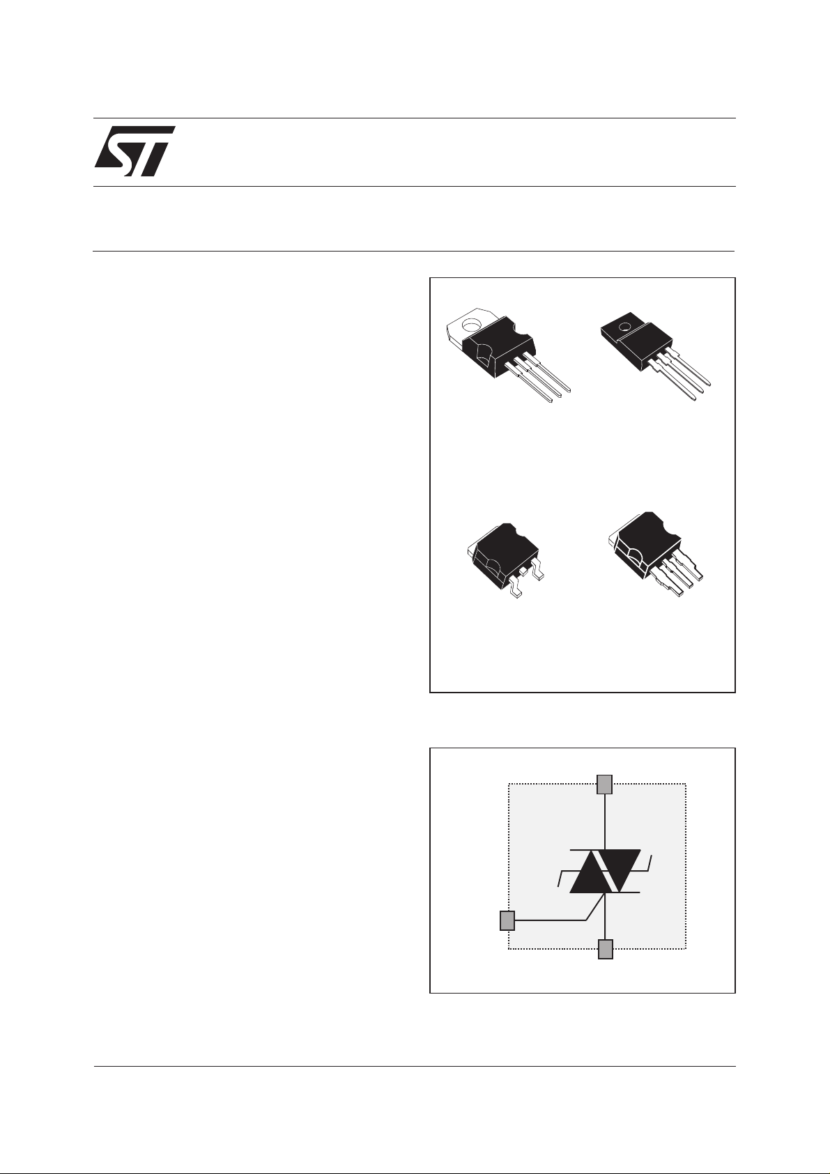
TO-220AB
ACST6-7ST
OUT
G
COM
D2PAK
ACST6-7SG
FUNCTIONAL DIAGRAM:
TO-220FPAB
ACST6-7SFP
OUT
I2PAK
ACST6-7SR
OUT
DESCRIPTION
The ACST6-7Sx belongs to the AC power switch
family built around the ASD technology. This high
performance device is adapted to home appliances
or industrial systems and drives an induction motor
up to 6A.
This ACST switch embeds a triac structure with a
high voltage clamping device to absorb the inductive
turn-off energy and withstand line transients such as
those described in the IEC61000-4-5 standards.
January 2002 - Ed: 7F
G
COM
1/9

ACST6-7S
ABSOLUTE RATINGS (limiting values)
Symbol Parameter Value Unit
V
DRM /
V
RRM
I
T(RMS)
I
TSM
2
I
t Thermal constraint for fuse selection tp = 10ms 11 A2s
dI/dt Non repetitive on-state current critical rate of rise
V
PP
Tstg Storage temperature range - 40 to + 150 °C
Tj Operating junction temperature range - 30 to + 125 °C
Tl Maximum lead soldering temperature during 10s 260 °C
Note 1:accordingto test described by IEC61000-4-5 standard & Figure A.
Repetitive peak off-state voltage Tj = 125 °C 700 V
RMS on-state current full cycle sine wave 50 to 60 Hz,
Tamb = 40 °C 1.5 A
no heat sink
RMS on-state current full cycle sine wave 50 to 60 Hz,
Tcase= 105 °C 6 A
TO-220AB package
Non repetitive surge peak on-state current
Tj initial = 25°C, full cycle sine wave
tp = 20ms 45 A
tp = 16.7ms 50 A
Rate period > 1mn 100 A/µs
I
= 10mA (tR< 100ns)
G
Non repetitive line peak pulse voltage
note 1
2kV
GATE CHARACTERISTICS (maximum values)
Symbol Parameter Value Unit
P
P
G (AV)
GM
I
GM
Average gate power dissipation 0.1 W
Peak gate power dissipation (tp = 20µs) 10 W
Peak gate current (tp = 20µs) 1 A
THERMAL RESISTANCE
Symbol Parameter Value Unit
Rth (j-a) Junction to ambient TO-220AB / TO-220FPAB 60 °C/W
Rth (j-a) Junction to ambient I
Rth (j-a) Junction to ambient D
Rth (j-c) Junction to case for full cycle sine wave conduction (TO-220AB) 2.5 °C/W
Rth (j-c) Junction to case for full cycle sine wave conduction (TO-220FPAB) 3.5 °C/W
2
PAK 65 °C/W
2
PAK soldered on 1cm2copper pad 45 °C/W
2/9

PARAMETER DESCRIPTION
Parameter Symbol Parameter description
ACST6-7S
I
GT
V
GT
V
GD
I
H
I
L
V
TM
V
TO
R
D
I
DRM/IRRM
Gate triggering current
Gate triggering voltage
Non triggering voltage
Holding current
Latching current
On state voltage
On state characteristic threshold voltage
On state characteristic dynamic resistance
Forward or reverse leakage current
dV/dt Static pin OUT voltage rise
(dI/dt)c Turn off current rate of decay
V
CL
Avalanche voltage at turn off
ELECTRICAL CHARACTERISTICS PER SWITCH
For either positive or negative polary of pin OUT voltage in respect to pin COM voltage
Symbol Test conditions Values Unit
I
GT
Vout = 12V (DC) RL=33Ω Tj = 25°C MAX. 10 mA
V
V
V
V
V
R
I
DRM
I
RRM
GT
GD
I
H
I
L
TM
TM
to
D
Vout= 12V (DC) RL=33Ω Tj = 25°C MAX. 1.5 V
V
OUT=VDRM
I
= 100mA Gate open Tj = 25°C MAX. 25 mA
OUT
RL= 3.3kΩ Tj =125°C MIN. 0.2 V
IG= 20mA Tj = 25°C MAX. 50 mA
I
= 2.1A tp = 380µs Tj = 25°C MAX. 1.4 V
OUT
I
= 8.5A tp = 380µs Tj = 25°C MAX. 1.7 V
OUT
Tj = 125°C MAX. 0.9 V
Tj = 125°C MAX. 80 mΩ
V
OUT=VDRM
V
OUT=VRRM
Tj = 25°C MAX. 20 µA
Tj = 125°C MAX. 500 µA
dV/dt V
= 600V gate open Tj = 125°C MIN. 200 V/µs
OUT
(dI/dt)c (dV/dt)c= 15V/µs Tj = 125°C MIN. 3 A/ms
(dI/dt)c (dV/dt)c= 15V/µs Iout < 0 Rgk = 150Ω Tj= 125°C MIN. 3.5 A/ms
V
CL
ICL= 1mA tp = 1ms Tj = 25°C TYP. 1100 V
3/9
 Loading...