®
ASD™
ACS402-5SB4
AC Switch Family
QUAD AC LINE SWITCH ARRAY
MAIN APPLICATIONS
AC Line switch for appliance control systems
n
Drive of low power high inductive or resistive
n
loads like:
- solenoid, relay, valve, dispenser
- micro-motor
- door lock
- low power lamp bulb
- pump
- fan
FEATURES
4 high voltage AC switch array
n
V
n
DRM/VRRM
Avalanche controlled device
n
I
n
T(RMS)
I
n
n
n
) = 0.4 A for the total array
T(RMS
Gate triggering current : IGT<10mA
Switch integrated driver
= 500V
PIN OUT CONNECTION
= 0.2 A per switch
OUT1
OUT2
BENEFITS
n
Miniaturizes 4 switches in 1 package.
n
Reducestheswitchcomponentcountbyupto80%.
n
Needs no more external protection snubber &
OUT3
OUT4
varistor.
n
Enables the equipment to meet IEC1000-4-5
standard.
n
Interfaces directly with the microcontroller.
n
Eliminates any stressing gate kick back on the
note : pins 1, 3, 5, 7, 9, 12, 14, 16, 18, 20 not connected.
microcontroller.
DESCRIPTION
The ACS402belongstotheAClineswitchesarray
family built around the ASD™ concept. This high
performance planar technology device includes 4
bi-directional a.c. switches able to control an 0.2 A
resistive or inductive load.
Each ACS™ switch integrates a high voltage
clamping structure to absorb the inductive turn off
energy and a gate level shifter driver to separate
the digital controller from each main switch. It is
triggered with a negative gate current flowing out
of the gate pin.
Note:
For further technical information, please refer to the Application note AN1172
DIL20
1
G1
G2
G3
G4
COMCOM
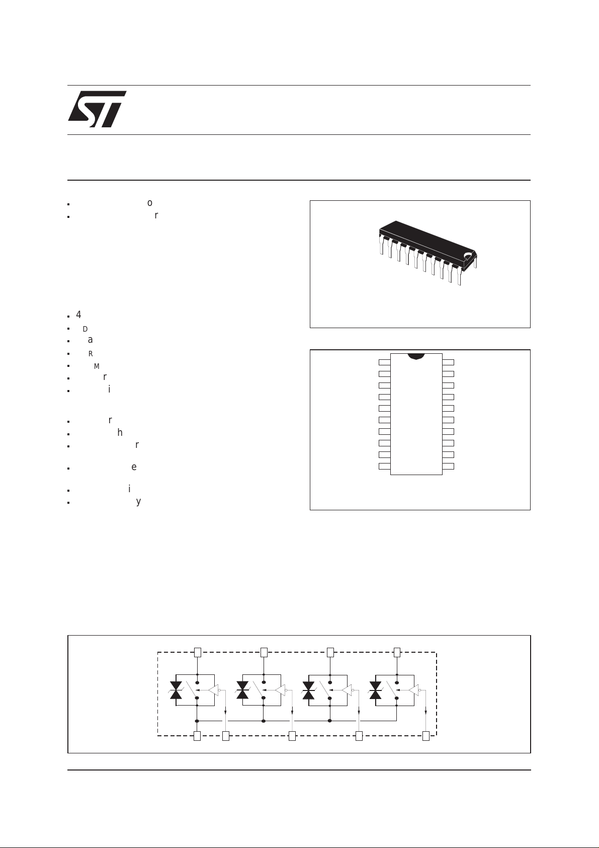
FUNCTIONAL DIAGRAM
ACS402
D1
November 1999 - Ed: 3B
S1
Com
OUT1
ON
D2
G1 G2 G3 G4
OUT2
S2
ON
D3
OUT3
S3
ON
S4
D4
OUT4
ON
1/6

ACS402-5SB4
ABSOLUTE RATINGS (limiting values)
Symbol Parameter Value Unit
V
DRM
V
RRM
I
T(RMS)
I
TSM
dI/dt Critical rate of rise of on-state current
V
PP
Tstg Storage temperature range - 40 to + 150 °C
Tj Operating junction temperature range 0 to + 110 °C
Tl Maximum lead temperature for soldering during 10s 260 °C
note 1 : according to test described by IEC 1000-4-5 standard & Figure 3.
SWITCH GATE CHARACTERISTICS (maximum values)
Symbol Parameter Value Unit
P
G (AV)
I
GM
V
GM
Repetitive peak off-state voltage Tj = 25 °C 500 V
RMS on-state current full cycle sine
wave 50 to 60 Hz
Non repetitive surge peak on-state current
Tj initial = 25°C, full cycle sine wave
= 20mA with tr = 100ns
I
G
Non repetitive line peak pulse voltage
per switch Tamb = 90 °C 0.2 A
total array Tamb = 75 °C 0.4 A
F =50 Hz 5 A
F =60 Hz 5.5 A
Repetitive
20 A/µs
F =120 Hz
note 1
2kV
Average gate power dissipation 0.1 W
Peak gate current (tp = 20µs) 1 A
Peak positive gate voltage (respect to the pin COM) 5 V
THERMAL RESISTANCE
Symbol Parameter Value Unit
Rth (j-a) Junction to ambient 90 °C/W
ELECTRICAL CHARACTERISTICS PER SWITCH
For either positive or negative polarity of pin OUT1, OUT2, OUT3, OUT4 voltage respect to pin COM voltage
Symbol Test conditions Values Unit
I
V
V
V
I
DRM
I
RRM
GT
I
I
GT
GD
H
L
TM
VD= 12V (DC) RL= 140Ω Tj=25°C MAX 10 mA
VD= 12V (DC) RL= 140Ω Tj=25°C MAX 1 V
V
OUT=VDRMRL
I
= 100mA gate open Tj=25°C TYP 25 mA
OUT
= 3.3kΩ Tj=110°C MIN 0.2 V
MAX 60 mA
IG= 20mA Tj=25°C TYP 30 mA
MAX 65 mA
I
= 0.3A tp= 380µs Tj=25°C MAX 1.1 V
OUT
V
OUT=VDRM
V
OUT=VRRM
Tj=25°C MAX 2 µA
Tj=110°C MAX 50 µA
dV/dt V
(dI/dt)c (dV
V
CL
2/6
= 400V gate open Tj=110°C MIN 500 V/µs
OUT
/dt)c = 10V/µs Tj=110°C MIN 0.1 A/ms
OUT
ICL= 1mA tp = 1ms Tj=25°C TYP 600 V
 Loading...