

SGS Thomson Microelectronics ACS302-5T3 Datasheet

®
ASD™
AC Switch Family
MAIN APPLICATIONS
AC on-off static switching in appliance &
■
industrial control systems
Drive of low power high inductive or resistive
■
loads like:
- relay, valve, solenoid, dispenser
- pump, fan, micro-motor
- low power lamp bulb, door lock
FEATURES
THREE HIGH VOLTAGE AC SWITCH ARRAY
■
BLOCKING VOLTAGE: V
■
CLAMPING VOLTAGE: VCL= 600 V
■
NOMINALCONDUCTINGCURRENTPERLINE:
■
T(RMS)
= 0.2 A
I
NOMINAL CONDUCTING CURRENT FOR
■
DRM/VRRM
TOTAL ARRAY:
T(RMS)
= 0.4 A
I
■ GATE TRIGGERING CURRENT: I
BENEFITS
■ Needs no external overvoltage protection
■
Enables equipment to meet IEC61000-4-5
standard
■
Interfaces directly with a microcontroller
■
Eliminates any stressing gate kick back on the
microcontroller
■
Array structure: design simplified, increase
reliability and space saving aspects
■
Mounting in SO-20 package enables the device
to meet IEC335-1 standard
<5mA
GT
= 500V
ACS302-5T3
THREE LINES AC SWITCH ARRAY
SO-20
Wired package
PIN-OUT
11.2cm = 2.54’’
OUTPUT 1 COM
OUTPUT 2
OUTPUT 3
1
2
3
4
5
6
7
8
9
10
8.5cm
20
19
18
17
16
15
14
13
12
11
GATE 1
GATE 2
3.81cm = 1.5’’
GATE 3
2.54cm = 1’’
COM
Pin 11
Pin 1
Pins 2, 3, 4, 6, 7, 8, 10,
and 19, 17, 15, 14, 12
.are not connected
DESCRIPTION
The ACS302 belongs to the AC line switch family
built around the ASD™ concept. This high
performance device inludes 3 bidirectionnal AC
switches able to control an 0.2A resistive or
inductive load device.
Each ACS™ switch embeds a high voltage
clamping structure to absorb the inductive turn off
energy and a gate level shifter driver to separate
the digital controller from the main switch. It is
triggered with a negative gate current flowing out
of the gate pin.
ASD and ACS are trademarks of STMicroelectronics.
January 2003 - Ed: 2
FUNCTIONAL DIAGRAM
OUT1 OUT2 OUT3
ACS302
S1 S2 S3
COM G1 G2 G3
1/8
ACS302-5T3
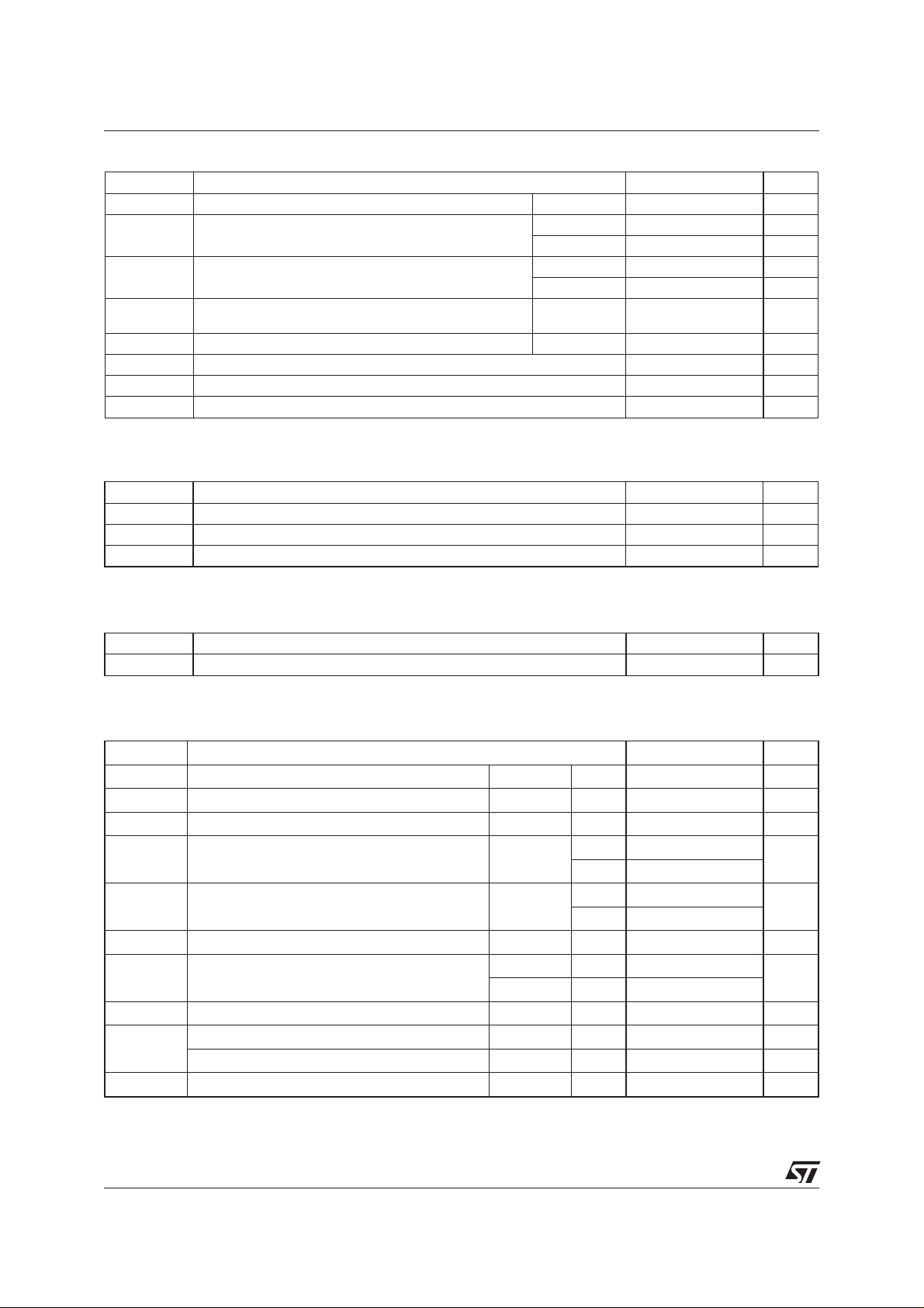
ABSOLUTE RATINGS (limiting values)
Symbol Parameter Value Unit
V
DRM/VRRM
I
T(RMS)
I
TSM
dI/dt Critical rate of repetitive rise of on-state current
V
PP
Tstg Storage temperature range - 40 to + 150 °C
Tj Operating junction temperature range - 30 to + 125 °C
Tl Maximum lead temperature for soldering during 10s 260 °C
Note 1: according to test described by IEC61000-4-5 standard and figure 3.
SWITCH GATE CHARACTERISTICS (maximum values)
Symbol Parameter Value Unit
P
G (AV)
I
GM
V
GM
Repetitive peak off-state voltage Tj = 125 °C 500 V
RMS on-state current full cycle sine wave 50 to 60 Hz Tamb = 110 °C One switch on = 0.2 A
Tamb = 90 °C Array: 0.4 A
Non repetitive surge peak on-state current
Tj initial = 25°C, full cycle sine wave
F =50 Hz 7.3 A
F =60 Hz 7.6 A
F =120 Hz 20 A/µs
I
= 10mA with tr = 100ns
G
Non repetitive line peak pulse voltage
note 1
2kV
Average gate power dissipation 0.1 W
Peak gate current (tp = 20µs) 1 A
Peak positive gate voltage (respect to the pin COM) 5 V
THERMAL RESISTANCES
Symbol Parameter Value Unit
Rth (j-a) Junction to ambient 93 °C/W
ELECTRICAL CHARACTERISTICS
Symbol Test Conditions Values Unit
V
I
GT
V
GT
V
GD
I
H
I
L
V
TM
I
DRM
I
RRM
dV/dt V
(dI/dt)c (dV/dt)c= 5V/µsI
V
CL
= 12V RL= 140Ω Tj=25°C MAX 5 mA
OUT
V
= 12V RL= 140Ω Tj=25°C MAX 0.9 V
OUT
V
OUT=VDRMRL
I
= 100mA gate open Tj=25°C TYP 20 mA
OUT
= 3.3kΩ Tj=125°C MIN 0.15 V
MAX 45
IG= 10mA Tj=25°C TYP 25 mA
MAX 50
I
= 0.3A tp = 380µs Tj=25°C MAX 1.2 V
OUT
V
OUT=VDRM
V
OUT=VRRM
= 400V gate open Tj=110°C MIN 300 V/µs
OUT
> 0 Tj=110°C MIN 0.1 A/ms
OUT
(dV/dt)c = 10V/µs I
< 0 Tj=110°C MIN 0.15 A/µs
OUT
Tj=25°C MAX 2 µA
Tj=125°C MAX 200
ICL= 1mA tp = 1ms Tj=25°C TYP 600 V
2/8

ACS302-5T3
ELECTRICAL CHARACTERISTICS
Symbol Parameter
I
GT
V
GT
V
GD
I
H
I
L
V
TM
V
t0
R
d
I
DRM/IRRM
dV/dt Critical rate of rise of off-state voltage
(dV/dt)
(dI/dt)
V
CL
I
CL
Triggering gate current
Triggering gate voltage
Non-triggering gate voltage
Holding current
Latching current
Peak on-state voltage drop
On-state threshold voltage
On-state dynamic resistance
Maximum forward or reverse leakage
current
Critical rate of decrease of commutating
c
off-state voltage
Critical rate of decrease of commutating
c
on-state current
Clamping voltage
Clamping current
AC LINE SWITCH BASIC APPLICATION
The ACS302 device is well adapted to washing
machines, dishwashers, tumble driers, refrigerators, water heaters, and cookwares. It has been
designed especially to switch ON & OFF low
power loads such as solenoids, valves, relays, micro-motors, pumps, fans, door locks and low
power lamp bulbs.
Pin COM: Common drivereference, to connect
■
to the power line neutral
Pin G: Switch Gate inputto connect to the digital
■
controller through a resistor
Pin OUT: Switch Output, to connect to the load
■
Each ACS™ switch is triggered with a negative
gate current flowing out of thegate pin G. It can be
driven directly by the digital controller through a
resistor as shown on the typical application
diagram. No protection devices are required
between the gates and common terminals.
In appliances systems, this ACS™ switch intends to drive low power loads in full cycle ON / OFF mode.
Thanks to its thermal and turn off commutation performances, the ACS302-5TA switch is able to drive
threeloads up to 0.2A each,as, for example, two watervalves and a door lockin a dishwasher, without any
additionnal turn-off snubber.
TYPICAL APPLICATION DIAGRAM
VALVE / DISPENSER DOOR LOCK PUMP / FAN
L
MAINS
N
ACS302
OUT1 OUT2 OUT3
S1 S2 S3
COM G1 G2 G3
PA0 PA 1 PA2
Vcc
Vss
ST72 MCU
M
3/7
 Loading...