

SGS Thomson Microelectronics 74VHCT16374ATTR Datasheet
1/10February 2003
■ HIGH SPEED:
f
MAX
= 185 MHz (TYP.) at VCC=5V
■ LOW POWER DISSIPATION:
I
CC
=4µA (MAX.) at TA=25°C
■ COMPATIBLE WITHTTL OUTPUTS:
V
IH
=2V (MIN.) VIL= 0.8 (MAX.)
■ POWER DOWN PROTECTION ON INPUTS
■ SYMMETRICAL OUTPUT IMPEDANCE:
|I
OH
|=IOL=8mA(MIN)
■ BALANCED PROPAGATION DELAYS:
t
PLH
≅ t
PHL
■ OPERATING VOLTAGE RANG E:
V
CC
(OPR) = 4.5V to 5.5V
■ PIN AND FUNCTION COMPATIBLE WITH
74 SERIES 16374
■ IMPROVED LATCH-UP IMMUNITY
■ LOW NOISE: V
OLP
= 0.9V (MAX.)
DESCRIPTION
The 74VHCT16374A is an advanced high-speed
CMOS 16 D-TYPE FLIP FLOP with 3 STATE
OUTPUTS NON INVERTING fabricated with
sub-micron silicon gate and double-la yer metal
wiring C
2
MOS technology.
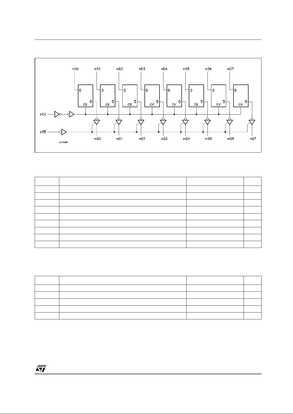
These 16 bit D-TYPE flip-flop is controlled by two
clock inputs (CK) and tw o output enable inputs
(nOE
). The device c an be us ed as two 8-bit
flip-flops or one 16-bit f lip -flop.
On t he positive trans ition of the clock, the Q
outputs will be set to the logic s tate that were
setup at the D inputs.
While the (OE
) input is low , the o utp uts will be in
a normal logic state (high or low logic level); while
OE
is high, the outputs will be in a high impedance
state.
The output con trol does no t affect the internal operation of flip-flops; that is, the old data can be retained or the new data can be entered even while
the outputs are off.
Power down protection is provided on all inputs
and 0 t o 7V can be accepted on inputs with no
regard to t he supply voltage. This device can be
usedto interface 5V to 3V.
All inputs and outpu ts are equipped with protection circuits against static discharge, giving them
2KV ESD immunity and transient excess vo ltage.
74VHCT16374A
16-BIT D-TYPE FLIP FLOP
WITH 3-STATE OUTPUTS NON INVERTING
ORDER CODES
PACKAGE TUBE T & R
TSSOP 74VHCT16374ATTR
TSSOP
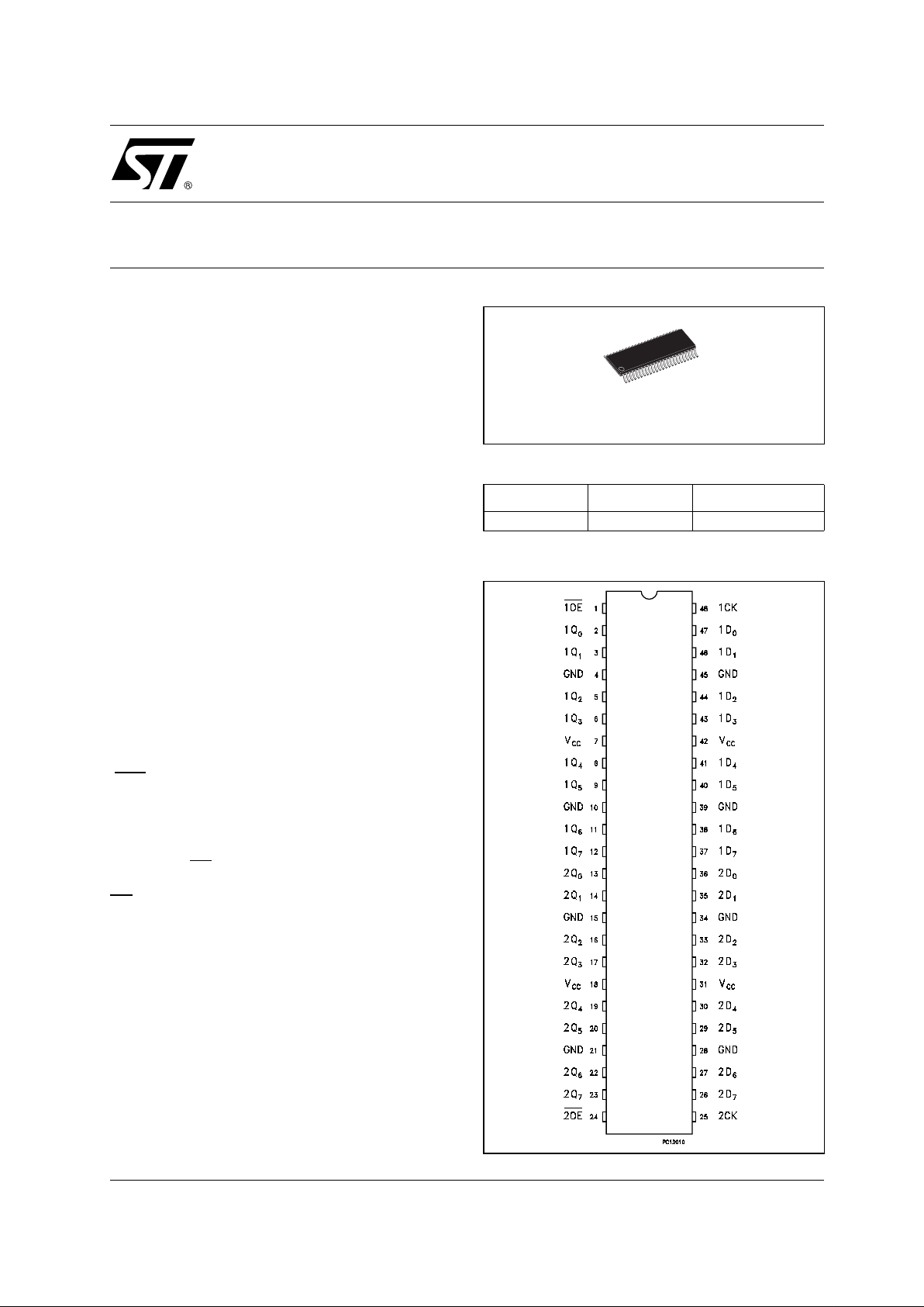
PIN CONNECTION
74VHCT16374A
2/10
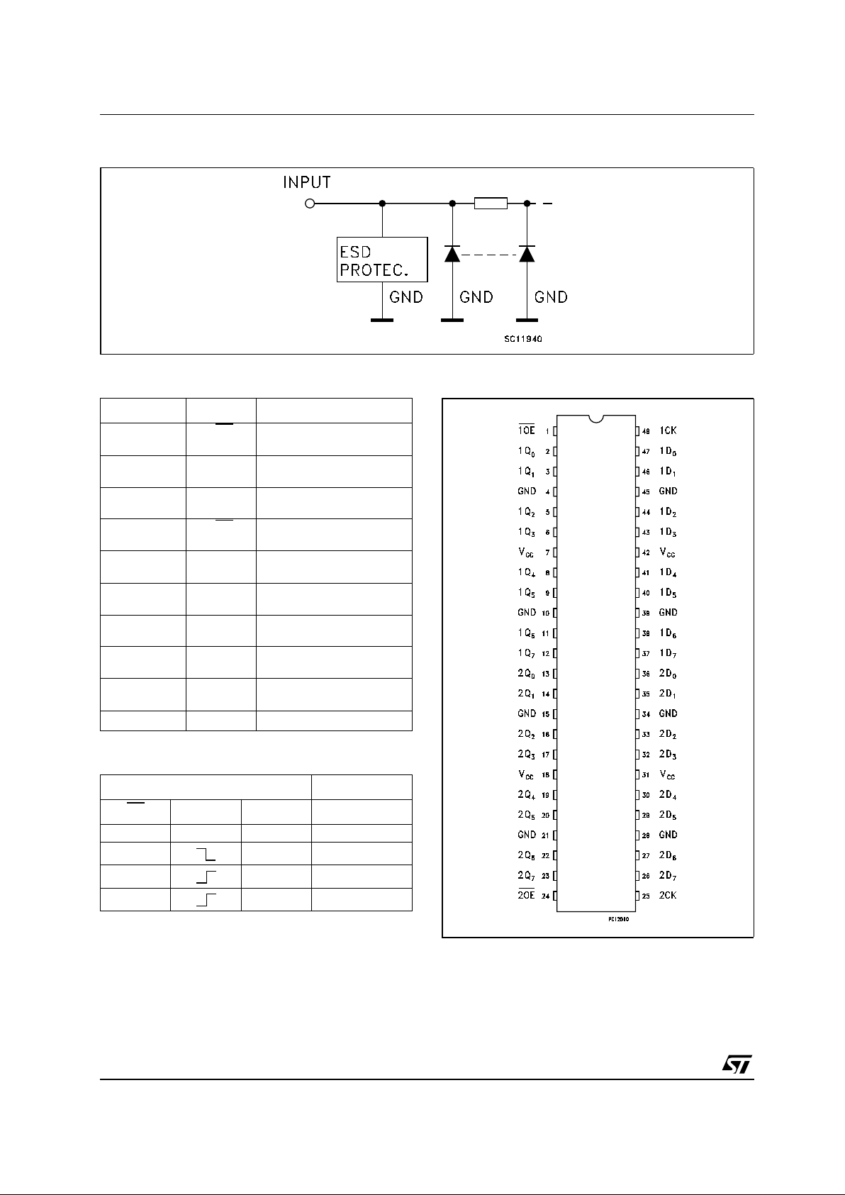
INPUT EQUIVALENT CIRCUIT
PIN DESCRIPTION
TRUTH TABLE
X : Don’tCare
Z : High Impedance
IEC LOGIC SYMBOLS
PIN No SYMBOL NAME AND FUNCTION
1 1OE
3 State Output Enable
Input (Active LOW)
2, 3,5, 6,8,9,
11, 12
1Q0 to
1Q7
3-State Outputs
13,14,16,17,
19, 20, 22, 23
2Q0 to
2Q7
3-State Outputs
24 2OE
3 State Output Enable
Input (Active LOW)
25 2CK Clock Input (LOW-to-HIGH
Edge Trigger)
36,35,33,32,
30, 29, 27, 26
2D0 to 2D7 Data Inputs
47,46,44,43,
41, 40, 38, 37
1D0 to 1D7 Data Inputs
48 1CK Clock Input (LOW-to-HIGH
Edge Trigger)
4, 10, 15, 21,
28, 34, 39, 45
GND Ground (0V)
7, 18, 31, 42 V
CC
Positive Supply Voltage
INPUTS OUTPUTS
OE
CK D Q
HXX Z
L X NO CHANGE
LLL
LHH
74VHCT16374A
3/10
LOGIC DIAGRAM
This logic diagram has not to be used to estimate propagation delays
ABSOLUTE MAXIMUM RATINGS
Absolute Maximum Ratings are those values beyond which damage to the device may occur. Functional operation under these conditions is
not implied
RECOMMENDED OPERATING CONDITIONS
1) VINfrom0.8V to 2.0V
Symbol Parameter Value Unit
V
CC
Supply Voltage
-0.5 to +7.0 V
V
I
DC Input Voltage
-0.5 to +7.0 V
V
O
DC Output Voltage -0.5 to VCC+ 0.5
V
I
IK
DC Input Diode Current
-20 mA
I
OK
DC Output Diode Current
± 20 mA
I
O
DC Output Current
± 25 mA
I
CC
or I
GND
DC VCCor Ground Current
± 75 mA
T
stg
Storage Temperature
-65 to +150 °C
T
L
Lead Temperature (10 sec)
300 °C
Symbol Parameter Value Unit
V
CC
Supply Voltage
4.5 to 5.5 V
V
I
Input Voltage
0 to 5.5 V
V
O
Output Voltage 0 to V
CC
V
T
op
Operating Temperature
-55 to 125 °C
dt/dv Input Rise and Fall Time (note 1) (Vcc= 5.0±0.5V)
0 to 20 ns/V
 Loading...