

SGS Thomson Microelectronics 74VHCT14ATTR, 74VHCT14AMTR, 74VHCT14AM Datasheet

74VHCT14A
HEX SCHMITT INVERTER
■ HIGH SPEED: t
■ LOW POWER DISSIPATION:
I
= 2 µA (MAX.) at TA=25°C
CC
■ TYPI C AL HYSTERESIS : 0.7V a t V
■ POWER DOWN PROTECTION ON INPUT S
= 5.5 ns (TYP.) at VCC = 5V
PD
= 4.5V
CC
& OUTPUTS
■ SYMMETRICAL OUTPUT IMPED ANCE:
|I
| = IOL = 8 mA (MIN)
OH
■ BALANCED PROPAGATION DELAYS:
t
≅ t
PLH
■ OPERATING VOLTAGE RANGE:
V
CC
■ PIN AND FUNCTION COMPATIBLE WITH
PHL
(OPR) = 4.5V to 5.5V
74 SERIES 14
■ IMPROVED LATCH-UP IMMUNITY
■ LOW NOISE: V
= 0.8V (MAX.)
OLP
DESCRIPTION
The 74VHCT14A is an advanced high-speed
CMOS HEX SCHMITT INVERTER fabricated wi th
sub-micron silicon gate and double-layer metal
wiring C
2
MOS technology.
The internal circuit is composed of 3 stages
including buffer ou tput, which provides high no ise
immunity and stable output.
Power down protection is provided on all inputs
and outputs and 0 to 7V can be accepted on
TSSOPSOP
ORDER CODES
PACKAGE TUBE T & R
SOP 74VHCT14AM 74VHCT14AMTR
TSSOP 74VHCT14ATTR
inputs with no regard to the supply voltage. This
device can be us ed to interf ac e 5V to 3V since al l
inputs are equipped with TTL threshold.
Pin configuration and function are the same as
those of the 74VHC04 but the 74VHC14 has
hysteresis.
This together with its schmitt trigger function
allows it to be used on line receivers with slow
rise/fall input signals.
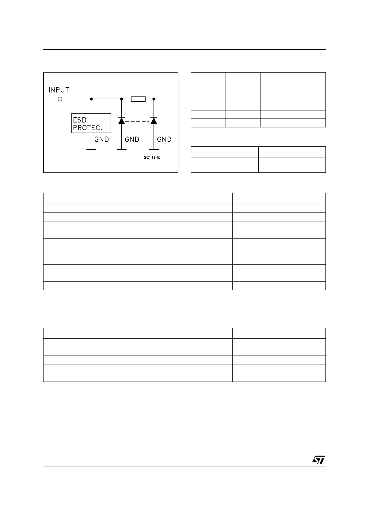
All inputs and outputs are equipped with
protection circuits against stat ic discharge, giving
them 2KV ESD immunity and transient excess
voltage.
PIN CONNECTION AND IEC LOGIC SYMBOLS
1/8June 2001
74VHCT14A
INPUT EQUIVALENT CIRCUIT PIN DESCRIPTION
PIN No SYMBOL NAME AND FUNCTION
1, 3, 5, 9, 1 1,
13
2, 4, 6, 8, 10,
12
7 GND Ground (0V)
14
TRUTH TABLE
ABSOLUTE MAXIMUM RATINGS
Symbol Parameter Value Unit
V
V
V
V
I
I
OK
I
I
or I
CC
T
T
Absolute Maximum Ratings are those values beyond which damage to the device may occur. Functional operation under these conditions is
not implied
1) V
CC
2) High or Low State
Supply Voltage
CC
DC Input Voltage
I
DC Output Voltage (see note 1)
O
DC Output Voltage (see note 2) -0.5 to VCC + 0.5
O
DC Input Diode Current
IK
DC Output Diode Current
DC Output Current
O
DC VCC or Ground Current
GND
Storage Temperature
stg
Lead Temperature (10 sec)
L
= 0V
1A to 6A Data Inputs
1Y to 6Y Data Outputs
V
CC
Positive Supply Voltage
AY
LH
HL
-0.5 to +7.0 V
-0.5 to +7.0 V
-0.5 to +7.0 V
V
- 20 mA
± 20 mA
± 25 mA
± 50 mA
-65 to +150 °C
300 °C
RECOMMENDED OPERATING CONDITIONS
Symbol Parameter Value Unit
V
V
V
V
T
1) V
CC
2) High or Low State
2/8
Supply Voltage
CC
Input Voltage
I
Output Voltage (see note 1)
O
Output Voltage (see note 2) 0 to V
O
Operating Temperature
op
= 0V
4.5 to 5.5 V
0 to 5.5 V
0 to 5.5 V
CC
-55 to 125 °C
V
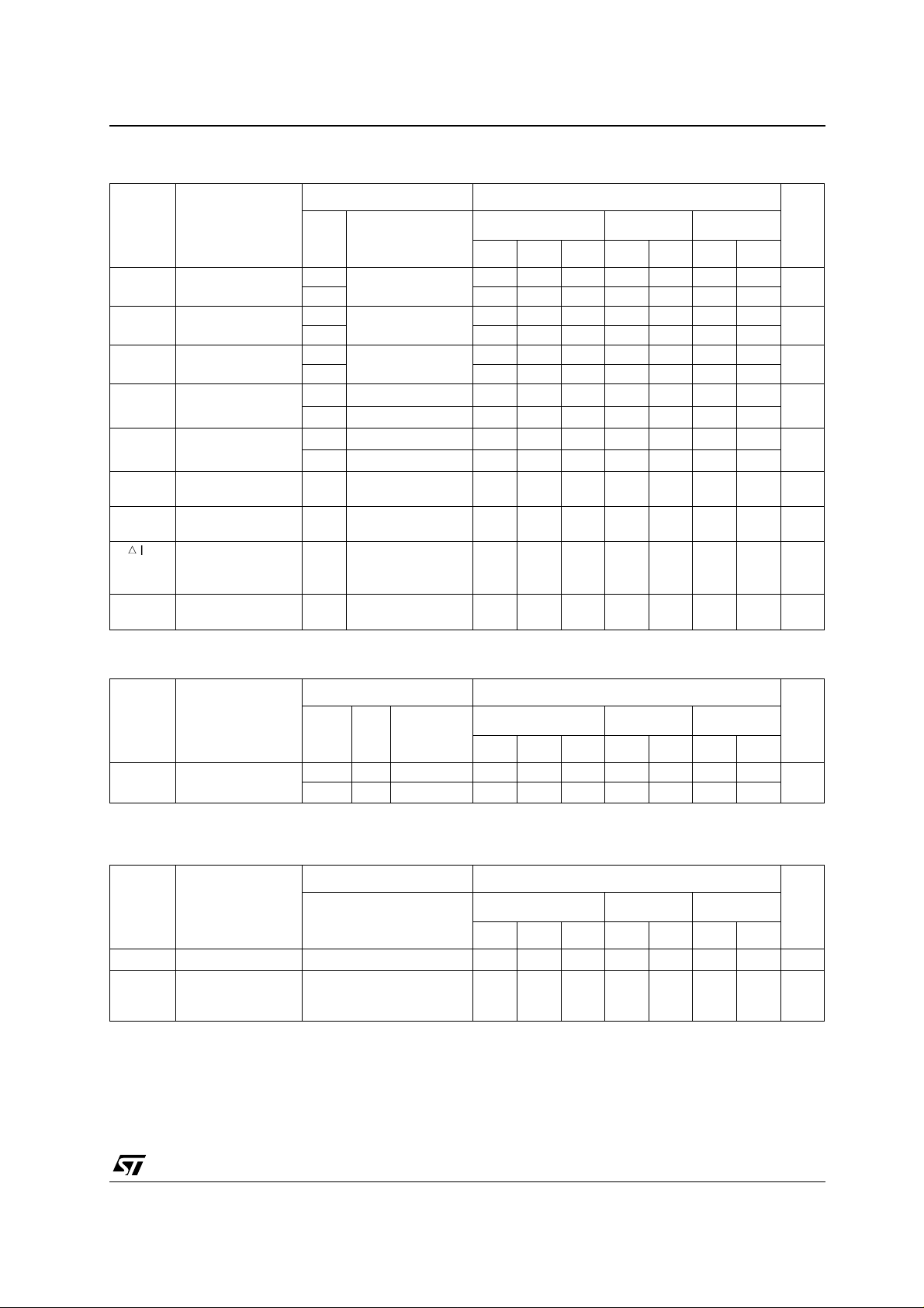
DC SPECIFICATIONS
Symbol Parameter
V
High Level
t+
Threshold Voltage
V
Low Level
t-
Threshold Voltage
V
Hysteresis Voltage 4.5 0.4 1.4 0.4 1.4 0.4 1.4
h
V
V
I
I
OPD
High Level Output
OH
Voltage
Low Level Output
OL
Voltage
I
Input Leakage
I
Current
Quiescent Supply
CC
Current
I
Additional Worst
CC
Case Supply
Current
Output Leakage
Current
74VHCT14A
Test Condition Value
T
= 25°C
V
CC
(V)
A
Min. Typ. Max. Min. Max. Min. Max.
4.5 2.0 2.0 2.0
5.5
2.0 2.0 2.0
4.5 0.6 0.6 0.6
5.5 0.6 0.6 0.6
5.5 0.4 1.5 0.4 1.5 0.4 1.5
4.5
4.5
4.5
4.5
0 to
5.5
5.5
IO=-50 µA
I
=-8 mA
O
IO=50 µA
=8 mA
I
O
V
= 5.5V or GND
I
= VCC or GND
V
I
4.4 4.5 4.4 4.4
3.94 3.8 3.7
0.0 0.1 0.1 0.1
One Input at 3.4V,
other input at V
5.5
CC
or GND
= 5.5V
0
V
OUT
-40 to 85°C -55 to 125°C
0.36 0.44 0.55
± 0.1 ± 1.0 ± 1.0 µA
22020µA
1.35 1.5 1.5 mA
0.5 5.0 5.0 µA
Unit
V
V
V
V
V
AC ELECTRICAL CHARACTERISTICS (Input t
= tf = 3ns)
r
Test Condition Value
= 25°C
Symbol Parameter
t
PLH
t
PHL
(*) Vol tage range is 5. 0V ± 0.5V
Propagation Delay
Time
(*)
(V)
C
(pF)
L
V
CC
5.0 15 5.5 8.6 1.0 10.0 1.0 10.0
5.0 50 6.7 9.0 1.0 11.0 1.0 11.0
T
A
-40 to 85°C -55 to 125°C
Min. Typ. Max. Min. Max. Min. Max.
Unit
ns
CAPACITIVE CHARACTERISTICS
Test Condition Value
= 25°C
Symbol Parameter
T
A
Min. Typ. Max. Min. Max. Min. Max.
C
C
Input Capacitance
IN
Power Dissipation
PD
Capacitance
6101010pF
16 pF
(note 1)
1) CPD is defined as the value of the IC’s internal equivalent capacitance which is calculated from the operating current consumption without
load. (Refer to Test Circuit). Average operating current can be obtained by the following equation. I
-40 to 85°C -55 to 125°C
= CPD x VCC x fIN + ICC/6 (per gate)
CC(opr)
Unit
3/8
 Loading...