SGS Thomson Microelectronics 74VHC374 Datasheet

WITH 3 STATE OUTPUT NON INVERTING
■ HIGHSPEED:
■ f
■ LOW POWER DISSIPATION:
■ HIGHNOISEIMMUNITY:
■ POWERDOWNPROTECTIONON INPUTS
■ SYMMETRICALOUTPUTIMPEDANCE:
■ BALANCEDPROPAGATIONDELAYS:
■ OPERATINGVOLTAGERANGE:
■ PINANDFUNCTIONCOMPATIBLEWITH
■ IMPROVEDLATCH-UP IMMUNITY
■ LOWNOISEV
DESCRIPTION
The 74VHC374 is an advanced high-speed
CMOS OCTAL D-TYPE FLIP FLOP with 3
STATE OUTPUT NON INVERTING fabricated
with sub-micron silicon gate and double-layer
metalwiring C
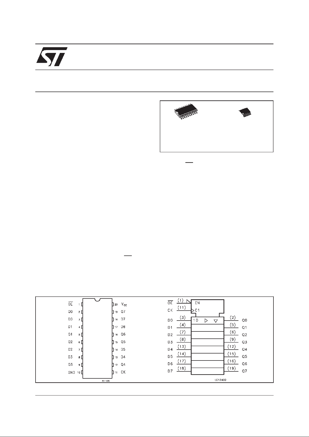
This 8 bit D-Type flip-flop is controlled by a clock
input (CK) and an outputenable input (OE).
On the positive transition of the clock, the Q
outputs will be set to the logic state that were
=270MHz(TYP.)atVCC=5V
MAX
=4 µA (MAX.)at TA=25oC
I
CC
V
NIH=VNIL
|I
|=IOL=8 mA(MIN)
OH
t
≅ t
PLH
(OPR)= 2Vto 5.5V
V
CC
=28%VCC(MIN.)
PHL
74SERIES374
=0.9V(Max.)
OLP
2
MOStechnology.
74VHC374
OCTAL D-TYPE FLIP FLOP
M
(Micro Package)
(TSSOPPackage)
ORDERCODES :
74VHC374M 74VHC374T
setupat the D inputs.
While the (OE) input is low, the 8 outputs will be
in a normal logic state (high or low logic level)
and while high level the outputs will be in a high
impedancestate.
The output control does not affect the internal
operation of flip flops; that is, the old data can be
retained or the new data can be entered even
whilethe outputsare off.
Power down protection is provided on all inputs
and 0 to 7V can be accepted on inputs with no
regard to the supply voltage. This device can be
used to interface 5V to 3V.
All inputs and outputs are equipped with
protection circuits against static discharge, giving
them 2KV ESD immunity and transient excess
voltage.
T
PIN CONNECTION AND IEC LOGICSYMBOLS
June 1999
1/10

74VHC374
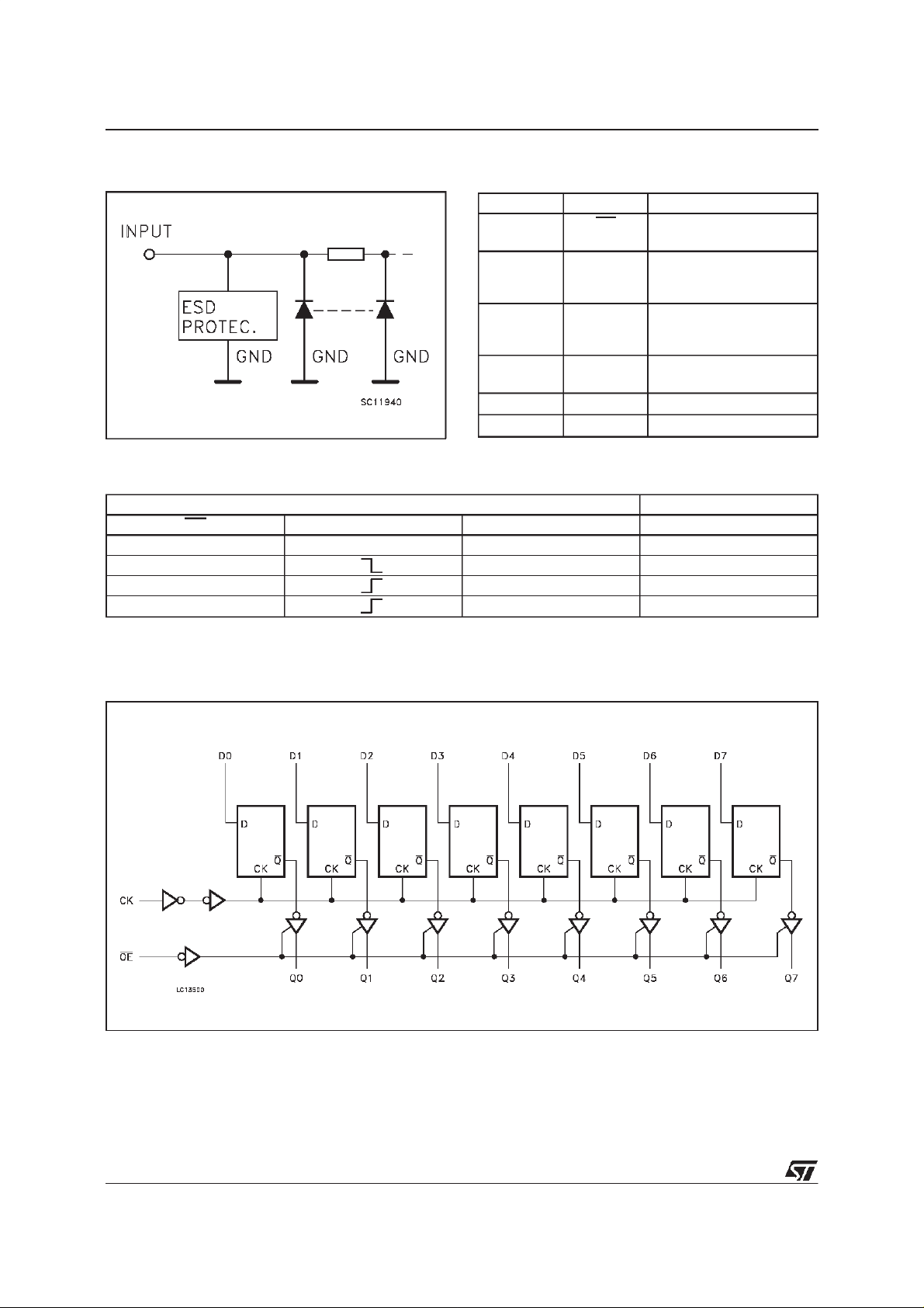
INPUT EQUIVALENTCIRCUIT PIN DESCRIPTION
PI N No SYMB OL NAME AND FU NCTION
1 OE 3 State Output Enable
2, 5, 6, 9,
12, 15, 16,
19
3, 4, 7, 8,
13, 14, 17,
18
11 CLOCK Clock Input (LOW to
10 GND Ground (0V)
20 V
TRUTH TABLE
INPUTS OUTPUTS
OE CK D Q
HXXZ
L X NO CHANGE
LLL
LHH
X:Don’tcare
Z:Highimpedance
Q0 to Q7 3 State Outputs
D0 to D7 Data Inputs
CC
Input (Active LOW)
HIGH, edge triggered)
Positive Supply Voltage
LOGICDIAGRAM
2/10

74VHC374
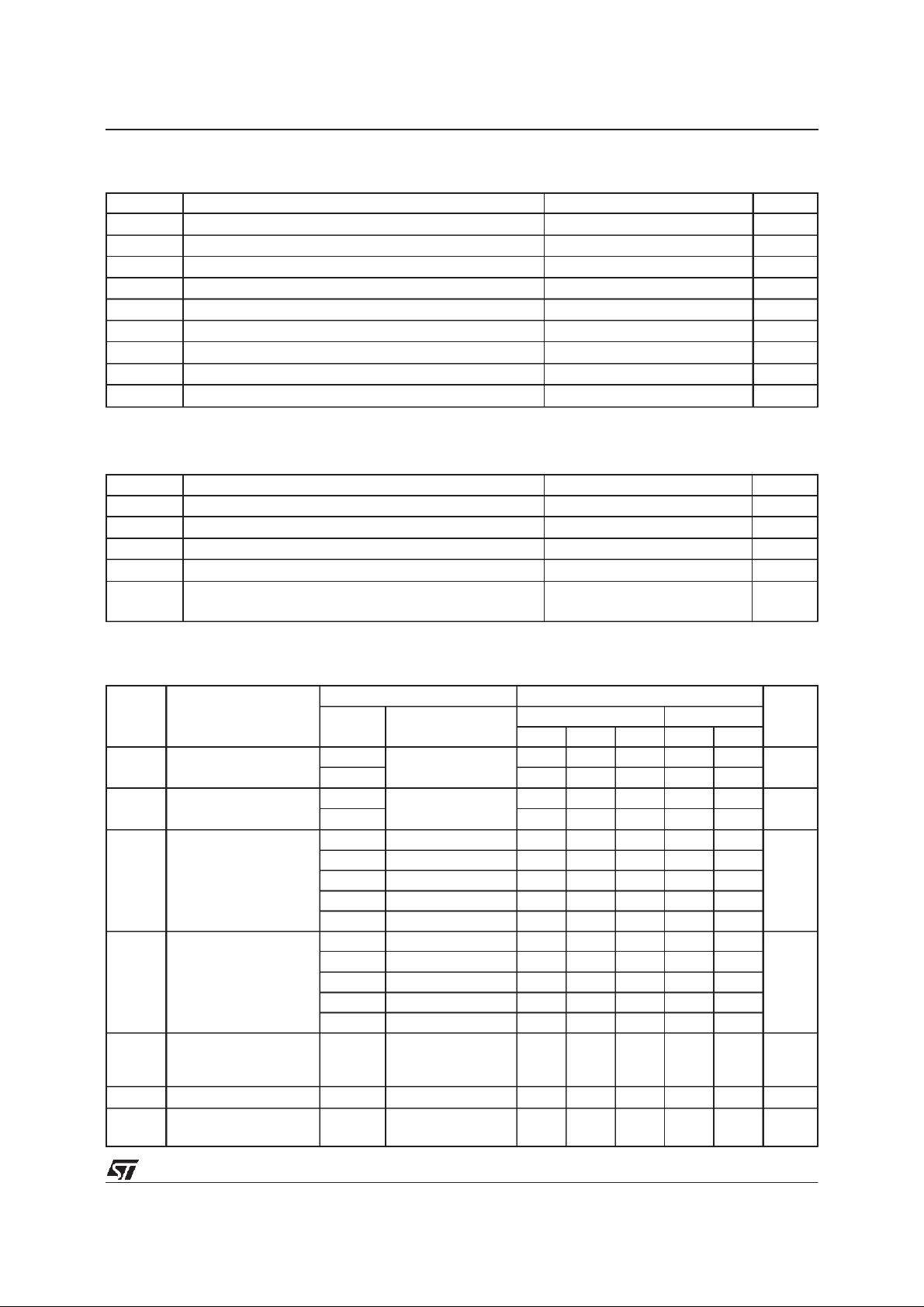
ABSOLUTE MAXIMUM RATINGS
Symb o l Para met er Val u e Uni t
V
V
V
I
I
OK
I
or I
I
CC
T
T
AbsoluteMaximumRatingsarethosevaluesbeyondwhichdamagetothedevicemayoccur. Functionaloperationunderthesecondition isnotimplied.
RECOMMENDEDOPERATINGCONDITIONS
Symb o l Para met er Value Un it
V
V
V
T
dt/dv
1)VINfrom30%to70%of V
Supply Voltage -0.5 to +7.0 V
CC
DC Input Voltage -0.5 to +7.0 V
I
DC Output Voltage -0.5 to VCC+ 0.5 V
O
DC Input Diode Current - 20 mA
IK
DC Output Diode Current ± 20 mA
DC Output Current
O
DC VCCor Ground Current
GND
Storage Temperature -65 to +150
stg
Lead Temperature (10 sec) 300
L
Supply Voltage 2.0 to 5.5 V
CC
Input Voltage 0 to 5.5 V
I
Output Voltage 0 to V
O
Operating Temperature -40 to +85
op
(V
CC
CC
=3.3±0.3V)
=5.0±0.5V)
Input Rise and Fall Time (see note 1) (V
CC
25 mA
±
75 mA
±
CC
0 to 100
0to20
o
C
o
C
V
o
C
ns/V
ns/V
DC SPECIFICATIONS
Symb o l Para met er Test C o n ditio ns Val u e Uni t
=25oC -40 to 85oC
V
CC
(V)
High Level Input
V
IH
Voltage
V
Low Level Input
IL
Voltage
V
High Level Output
OH
Voltage
2.0 1.5 1.5
3.0 to 5.5 0.7V
2.0 0.5 0.5
3.0 to 5.5 0.3V
2.0 IO=-50µA 1.9 2.0 1.9
3.0 I
4.5 I
3.0 I
4.5 I
Low Level Output
V
OL
Voltage
2.0 IO=50 µ A 0.0 0.1 0.1
3.0 I
4.5 I
3.0 I
4.5 I
High Impedance
I
OZ
Output Leakage
5.5
VO=VCCor GND
Current
Input Leakage Current 0 to5.5 VI= 5.5V or GND
I
I
Quiescent Supply
I
CC
5.5 VI=VCCorGND 4 40
Current
=-50µA 2.9 3.0 2.9
O
=-50 µA 4.4 4.5 4.4
O
=-4 mA 2.58 2.48
O
=-8 mA 3.94 3.8
O
=50µA 0.0 0.1 0.1
O
=50 µA 0.0 0.1 0.1
O
=4 mA 0.36 0.44
O
=8 mA 0.36 0.44
O
VI=VIHor V
IL
T
A
Min. Typ. Max. Min. Max.
CC
0.7V
CC
0.3V
CC
±0.25 ±2.5 µA
0.1
±
1.0
±
CC
µ
µ
V
V
V
V
A
A
3/10
 Loading...