

74VHC240
OCTAL BUS BUFFER
WITH 3 STATE OUTPUTS (INVERTED)
■ HIGHSPEED:t
■ LOW POWERDISSIPATION:
=4 µA (MAX.) at TA=25oC
I
CC
■ HIGHNOISEIMMUNITY:
V
NIH=VNIL
■ POWERDOWNPROTECTIONON INPUTS
■ SYMMETRICALOUTPUTIMPEDANCE:
|=IOL=8 mA (MIN)
|I
OH
■ BALANCEDPROPAGATIONDELAYS:
t
≅ t
PLH
■ OPERATINGVOLTAGERANGE:
V
(OPR)= 2Vto 5.5V
CC
■ PINANDFUNCTIONCOMPATIBLEWITH
=28%VCC(MIN.)
PHL
=3.6ns(TYP.)atVCC=5V
PD
74SERIES240
■ IMPROVEDLATCH-UP IMMUNITY
■ LOWNOISE:V
= 0.9V(Max.)
OLP
DESCRIPTION
The 74VHC240 is an advanced high-speed
CMOS OCTAL BUS BUFFER (3-STATE)
fabricated with sub-micron silicon gate and
double-layermetal wiring C
2
MOS technology.
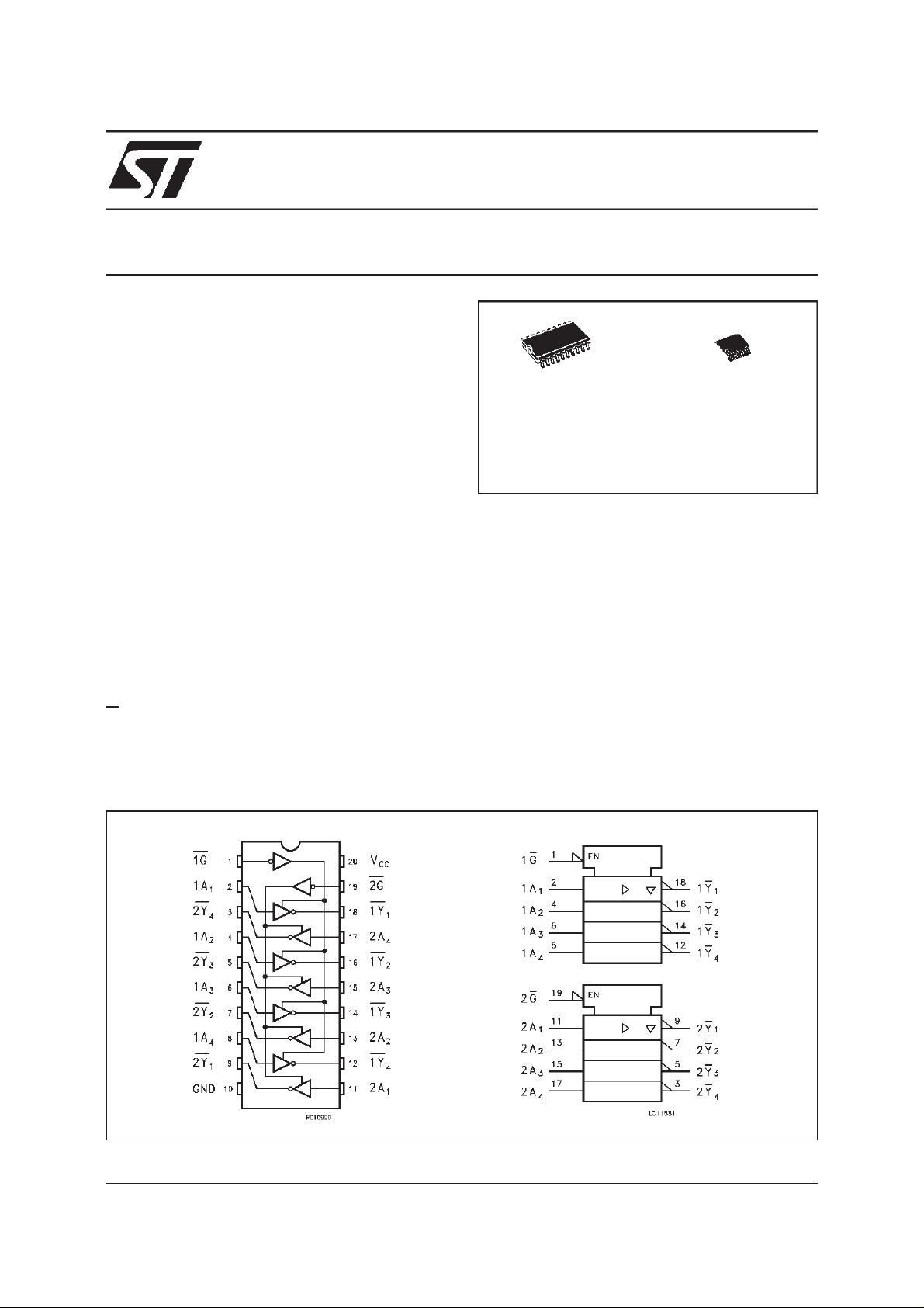
G output enable governsfour BUS BUFFERs.
M
(Micro Package)
(TSSOPPackage)
T
ORDERCODES :
74VHC240M 74VHC240T
This device is designed to be used with 3 state
memoryaddressdrivers, etc.
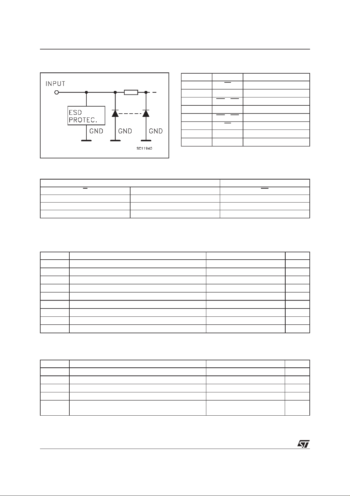
Power down protection is provided on all inputs
and 0 to 7V can be accepted on inputs with no
regard to the supply voltage. This device can be
used to interface5V to 3V.
All inputs and outputs are equipped with
protection circuits against static discharge, giving
them 2KV ESD immunity and transient excess
voltage.
PIN CONNECTIONAND IEC LOGIC SYMBOLS
June 1999
1/8
74VHC240
INPUT EQUIVALENTCIRCUIT
TRUTH TABLE
GAnYn
LLH
LHL
HXZ
X:”H” or”L”
Z:Highimpedance
PIN DESCRIPTION
PI N No SYM BO L NAM E AND F UNCT I ON
1 1G Output Enable Input
2,4,6,8 1A1to1A4 Data Inputs
9,7,5,3 2Y1to2Y4 Data Outputs
11,13,15,17 2A1to2A4 Data Inputs
18,16,14,12 1Y1to1Y4 Data Outputs
19 2G Output Enable Input
10 GND Ground (0V)
20 V
INPUT OUTPU T
Positive Supply Voltage
CC
ABSOLUTE MAXIMUM RATINGS
Symb o l Para met er Val u e Uni t
V
V
V
I
I
OK
I
orI
I
CC
T
T
AbsoluteMaximum Ratingsarethosevalues beyond whichdamagetothedevicemayoccur. Functionaloperationunder these condition isnotimplied.
Supply Voltage -0.5to+7.0 V
CC
DC Input Voltage -0.5to+7.0 V
I
DC Output Voltage -0.5toVCC+0.5 V
O
DC Input Diode Current -20 mA
IK
DC Output Diode Current ±20 mA
DC Output Current ±25 mA
O
DC VCCor Ground Current ±75 mA
GND
Storage Temperature -65to+150
stg
Lead Temperature (10 sec) 300
L
o
C
o
C
RECOMMENDEDOPERATINGCONDITIONS
Symb o l Para met er Value Un it
V
V
V
T
dt/dv
1)VINfrom30%to70%of V
Supply Voltage 2.0to5.5 V
CC
Input Voltage 0to5.5 V
I
Output Voltage 0toV
O
Operating Temperature -40to+85
op
(V
CC
CC
=3.3±0.3V)
=5.0±0.5V)
Input Rise and Fall Time (see note 1) (V
CC
CC
0to100
0to20
V
o
C
ns/V
ns/V
2/8
74VHC240
DC SPECIFICATIONS
Symb o l Para met er Test Con diti o ns Val u e Unit
T
V
CC
(V)
High Level Input
V
IH
Voltage
V
Low Level Input
IL
Voltage
V
High Level Output
OH
Voltage
2.0 1.5 1.5
3.0to 5.5 0.7V
2.0 0.5 0.5
3.0to 5.5 0.3V
2.0 IO=-50µA1.92.0 1.9
3.0 I
4.5 I
3.0 I
4.5 I
Low Level Output
V
OL
Voltage
2.0 IO=50µA 0.0 0.1 0.1
3.0 I
4.5 I
3.0 I
4.5 I
High Impedance
I
OZ
Output Leakage
5.5
Current
Input Leakage Current 0to5.5 VI=5.5Vor GND
I
I
Quiescent Supply
I
CC
5.5 VI=VCCorGND 4 40
Current
Min. Typ. Max. Min. Max.
=-50µA2.93.0 2.9
O
=-50µA4.44.5 4.4
O
=-4mA 2.58 2.48
O
=-8mA 3.94 3.8
O
=50µA 0.0 0.1 0.1
O
=50µA 0.0 0.1 0.1
O
=4mA 0.36 0.44
O
=8mA 0.36 0.44
O
VI=VIHorV
IL
VO=VCCorGND
=25oC -40 to 85oC
A
±
±
0.7V
CC
0.25
0.1
CC
CC
0.3V
±
±
2.5
1.0
CC
µ
µ
µ
V
V
V
V
A
A
A
AC ELECTRICALCHARACTERISTICS (Inputtr=tf=3 ns)
Symbol Parameter Test Conditi on Value Unit
t
Propagation Delay
PLH
t
Time
PHL
Output Enable Time 3.3
t
PZL
t
PZH
t
Output Disable Time 3.3
PLZ
t
PHZ
t
t
(*) Voltage rangeis3.3V ±0.3V
(**) Voltagerangeis 5V±0.5V
Note1:Parameterguaranteedbydesign. t
Output to Output Skew
OSLH
Time (note 1)
OSHL
soLH
V
(V)
3.3
3.3
5.0
5.0
3.3
5.0
5.0
5.0
3.3
5.0
=|t
pLHm-tpLHn
CC
C
L
(pF)
(*)
(*)
(**)
(**)
(*)
(*)
(**)
(**)
(*)
(**)
(*)
(**)
15 5.3 7.5 1.0 9.0
50 7.8 11.0 1.0 12.5
15 3.6 5.5 1.0 6.5
50 5.1 7.5 1.0 8.5
15 RL=1KΩ 6.6 10.6 1.0 12.5
50 RL=1K
15 RL=1KΩ 4.7 7.3 1.0 8.5
50 RL=1K
50 RL=1KΩ 10.3 14.0 1.0 16.0
50 RL=1K
50 1.5 1.5 ns
50
|,t
soHL
=|t
pHLm-tpHLn
|
Min. Typ. Max. Min. Max.
Ω
Ω
Ω
=25oC -40 to 85oC
T
A
9.1 14.1 1.0 16.0
6.2 9.3 1.0 10.5
6.7 9.2 1.0 10.5
1.0 1.0
ns
ns
ns
3/8

74VHC240
CAPACITIVE CHARACTERISTICS
Symb o l Para met er Test Con diti o ns Val u e Unit
=25oC -40 to 85oC
T
A
Min. Typ. Max. Min. Max.
Input Capacitance 4 10 10
C
IN
C
Output Capacitance 6
OUT
Power Dissipation
C
PD
17 pF
Capacitance (note 1)
1)CPDisdefinedasthevalue oftheIC’sinternalequivalentcapacitance whichis calculated fromtheoperatingcurrentconsumption withoutload. (Referto
TestCircuit).Average operatingcurrentcanbe obtained bythefollowingequation.I
(opr)=CPD• VCC• fIN+ICC/8(perCircuit)
CC
DYNAMICSWITCHING CHARACTERISTICS
Symb o l Para met er Test Con diti o ns Val u e Unit
T
V
CC
(V)
V
V
Dynamic Low Voltage
OLP
Quiet Output (note 1, 2)
OLV
Dynamic High Voltage
V
IHD
5.0
5.0 3.5
=50pF
C
L
Min. Typ. Max. Min. Max.
Input (note 1, 3)
Dynamic Low Voltage
V
ILD
5.0 1.5
Input (note 1, 3)
1)Worstcasepackage.
2)Maxnumberof outputs defined as(n).Datainputs aredriven0Vto5.0V,(n-1)outputs switching andoneoutputatGND.
3)Maxnumberof datainputs (n)switching.(n-1)switching0Vto5.0V. Inputsunder testswitching: 5.0Vtothreshold (V
=25oC -40 to 85oC
A
0.6 0.9
-0.9 -0.6
),0Vtothreshold (V
ILD
),f=1MHz.
IHD
pF
pF
V
TESTCIRCUIT
TEST SW ITCH
t
PLH,tPHL
t
PZL,tPLZ
t
PZH,tPHZ
CL= 15/50 pFor equivalent (includes jig and probe capacitance)
=1KΩorequivalent
R
L=R1
R
ofpulsegenerator (typically50Ω)
T=ZOUT
Open
V
CC
GND
4/8

74VHC240
WAVEFORM 1: PROPAGATIONDELAYS
(f=1MHz;50% duty cycle)
WAVEFORM 2: OUTPUTENABLEAND DISABLE TIME(f=1MHz; 50% duty cycle)
5/8

74VHC240
SO-20 MECHANICAL DATA
DIM.
MIN. TYP. MAX. MIN. TYP. MAX.
A 2.65 0.104
a1 0.10 0.20 0.004 0.007
a2 2.45 0.096
b 0.35 0.49 0.013 0.019
b1 0.23 0.32 0.009 0.012
C 0.50 0.020
c1 45 (typ.)
D 12.60 13.00 0.496 0.512
E 10.00 10.65 0.393 0.419
e 1.27 0.050
e3 11.43 0.450
F 7.40 7.60 0.291 0.299
L 0.50 1.27 0.19 0.050
M 0.75 0.029
S 8 (max.)
mm inch
6/8
P013L

TSSOP20 MECHANICAL DATA
74VHC240
DIM.
mm inch
MIN. TYP. MAX. MIN. TYP. MAX.
A 1.1 0.433
A1 0.05 0.10 0.15 0.002 0.004 0.006
A2 0.85 0.9 0.95 0.335 0.354 0.374
b 0.19 0.30 0.0075 0.0118
c 0.09 0.2 0.0035 0.0079
D 6.4 6.5 6.6 0.252 0.256 0.260
E 6.25 6.4 6.5 0.246 0.252 0.256
E1 4.3 4.4 4.48 0.169 0.173 0.176
e 0.65 BSC 0.0256 BSC
K0
o
o
4
o
8
o
0
o
4
L 0.50 0.60 0.70 0.020 0.024 0.028
o
8
A2
A
A1
PIN 1 IDENTIFICATION
b
e
K
c
L
E
D
E1
1
7/8

74VHC240
Information furnished is believed to be accurate and reliable. However, STMicroelectronics assumes no responsibility for the consequences
of use of such information nor for any infringement of patents or other rights of third parties which may result from its use. No license is
granted by implication or otherwise under any patent or patent rights of STMicroelectronics. Specification mentioned in this publication are
subject to change without notice. This publication supersedes and replaces all information previously supplied. STMicroelectronics products
are not authorized for use as critical components in life support devices or systems without express written approval of STMicroelectronics.
The ST logo is a trademarkof STMicroelectronics
1999 STMicroelectronics – Printed in Italy – All Rights Reserved
STMicroelectronics GROUP OF COMPANIES
Australia - Brazil - Canada - China -France - Germany - Italy - Japan - Korea -Malaysia - Malta - Mexico - Morocco - The Netherlands -
Singapore - Spain - Sweden - Switzerland - Taiwan - Thailand - UnitedKingdom - U.S.A.
http://www.st.com
.
8/8
 Loading...