

SGS Thomson Microelectronics 74VHC14 Datasheet
■ HIGHSPEED:t
■
LOW POWER DISSIPATION:
I
=2 µA (MAX.)at TA=25oC
CC
■
TYPICAL HYSTERESIS:Vh=1VatVCC=4.5V
■ POWERDOWNPROTECTIONON INPUTS
■ SYMMETRICALOUTPUTIMPEDANCE:
|=IOL=8 mA(MIN)
|I
OH
■ BALANCEDPROPAGATIONDELAYS:
t
≅ t
PLH
PHL
■ OPERATINGVOLTAGERANGE:
V
(OPR)= 2Vto5.5V
CC
■
PINANDFUNCTIONCOMPATIBLEWITH
=5.5ns(TYP.)atVCC=5V
PD
74SERIES14
■ IMPROVEDLATCH-UPIMMUNITY
■ LOWNOISE:V
= 0.8V(Max.)
OLP
DESCRIPTION
The 74VHC14 is an advanced high-speedCMOS
HEX SCHMITT INVERTER fabricated with
sub-micron silicon gate and double-layer metal
wiringC
2
MOStechnology.
The internal circuit is composed of 3 stages
including buffer output, which enables high noise
immunityand stableoutput.
Power down protection is provided on all inputs
and 0 to 7V can be accepted on inputs with no
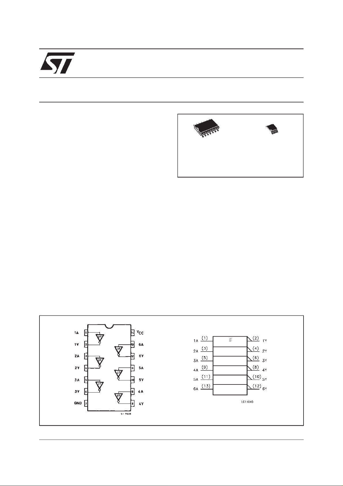
74VHC14
HEX SCHMITT INVERTER
PRELIMINARY DATA
M
(Micro Package)
(TSSOPPackage)
ORDERCODES :
74VHC14M 74VHC14T
regard to the supply voltage. This device can be
used to interface 5V to 3V.
Pin configuration and function are the same as
those of the VHC04 but the VHC14 has
hysteresis.
This together with its schmitt trigger function
allows it to be used on line receivers with slow
rise/fallinput segnals.
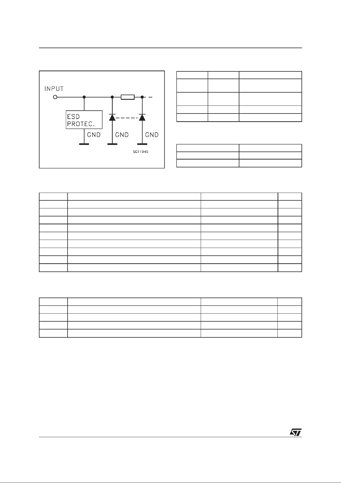
All inputs and outputs are equipped with
protection circuits against static discharge, giving
them 2kV ESD immunity and transient excess
voltage.
T
PIN CONNECTION AND IEC LOGICSYMBOLS
June 1999
1/7
74VHC14
INPUT EQUIVALENTCIRCUIT
PIN DESCRIPTION
PI N No SYMB OL NAME AND F U NCTIO N
1, 3, 5, 9,
1A to 6A Data Inputs
11, 13
2, 4, 6, 8,
1Y to 6Y Data Outputs
10, 12
7 GND Ground (0V)
14 V
CC
Positive Supply Voltage
TRUTH TABLE
AY
LH
HL
ABSOLUTE MAXIMUM RATINGS
Symb o l Para met er Val u e Uni t
V
V
V
I
I
OK
I
or I
I
CC
T
T
AbsoluteMaximumRatingsarethosevaluesbeyondwhichdamageto thedevicemayoccur.Functionaloperation underthesecondition isnotimplied.
Supply Voltage -0.5 to +7.0 V
CC
DC Input Voltage -0.5 to +7.0 V
I
DC Output Voltage -0.5 to VCC+ 0.5 V
O
DC Input Diode Current - 20 mA
IK
DC Output Diode Current
DC Output Current
O
DC VCCor Ground Current
GND
Storage Temperature -65 to +150
stg
Lead Temperature (10 sec) 300
L
20 mA
±
25 mA
±
50 mA
±
o
C
o
C
RECOMMENDED OPERATINGCONDITIONS
Symb o l Para met er Value Un it
V
V
V
T
2/7
Supply Voltage 2.0 to 5.5 V
CC
Input Voltage 0 to 5.5 V
I
Output Voltage 0 to V
O
Operating Temperature -40 to +85
op
CC
V
o
C
74VHC14
DC SPECIFICATIONS
Symb o l Para met er Test Con dit io ns Val u e Uni t
T
V
CC
High Level Threshold
V
t+
Voltage
(V)
3.0 2.2 2.2
4.5 3.15 3.15
Min. Typ. Max. Min. Max.
5.5 3.85 3.85
Low Level Threshold
V
t-
Voltage
3.0 0.9 0.9
4.5 1.35 1.35
5.5 1.65 1.65
Hysteresis Voltage 3.0 0.3 1.2 0.3 1.2
V
h
4.5 0.4 1.4 0.4 1.4
5.5 0.5 1.6 0.5 1.6
High Level Output
V
OH
Voltage
Low Level Output
V
OL
Voltage
Input Leakage Current 0 to 5.5 VI= 5.5V or GND
I
I
Quiescent Supply
I
CC
2.0 IO=-50µA 1.9 2.0 1.9
3.0 I
4.5 I
3.0 I
4.5 I
=-50 µA 2.9 3.0 2.9
O
=-50 µA 4.4 4.5 4.4
O
=-4 mA 2.58 2.48
O
=-8 mA 3.94 3.8
O
2.0 IO=50µA 0.0 0.1 0.1
3.0 I
4.5 I
3.0 I
4.5 I
=50µA 0.0 0.1 0.1
O
=50 µA 0.0 0.1 0.1
O
=4 mA 0.36 0.44
O
=8 mA 0.36 0.44
O
5.5 VI=VCCorGND 2 20
Current
=25oC -40 to 85oC
A
0.1
±
1.0
±
µ
µ
V
V
V
V
V
A
A
AC ELECTRICAL CHARACTERISTICS
(Inputt
r=tf
=3 ns)
Symbol Parameter Test Condition Value Unit
t
Propagation Delay
PLH
t
Time
PHL
(*) Voltagerangeis 3.3V± 0.3V
(**) Voltagerangeis 5V± 0.5V
V
3.3
3.3
5.0
5.0
CC
(V)
(**)
(**)
C
L
(pF)
(*)
(*)
15 8.3 12.8 1.0 15.0
50 10.8 16.3 1.0 18.5
T
=25oC -40 to 85oC
A
Min. Typ. Max. Min. Max.
ns
15 5.5 8.6 1.0 10.0
50 7.0 10.6 1.0 12.0
CAPACITIVE CHARACTERISTICS
Symb o l Para met er Test Con dit io ns Val u e Uni t
=25oC -40 to 85oC
T
A
Min. Typ. Max. Min. Max.
Input Capacitance 4 10 10
C
IN
Power Dissipation
C
PD
21 pF
Capacitance (note 1)
1)CPDisdefined asthevalue oftheIC’sinternal equivalentcapacitance whichis calculated fromtheoperatingcurrent consumptionwithout load.(Referto
TestCircuit).Average operatingcurrent canbeobtainedbythefollowingequation.I
(opr)= C
CC
•
•
f
IN+ICC
/6(perGate)
V
PD
CC
pF
3/7
 Loading...