

1/8June 2001
■ HIGH SPEED: t
PD
= 3.7ns (TYP.) at VCC = 5V
■ LOW POWER DISSIPATION:
I
CC
= 2 µA (MAX.) at TA=25°C
■ HIGH NOISE IMMUNITY:
V
NIH
= V
NIL
= 28% VCC (MIN.)
■ POWER DOWN PROTECTION ON INPUTS
■ OPERATING VOLTAGE RANGE:
V
CC
(OPR) = 2V to 5.5V
■ PIN AND FUNCTION COMPATIBLE WITH
74 SERIES 03
■ IMPROVED LATCH-UP IMMUNITY
■ LOW NOISE: V
OLP
= 0.8V (MAX.)
DESCRIPTION
The 74VHC03 is a n advanced high-speed CM OS
QUAD 2-INPUT OPEN DRAIN NAND GATE
fabricated with sub-micron silicon gate and
double-layer metal wiring C
2
MOS technology.
The internal circuit is composed of 3 stages
including buffer ou tput, which provides high no ise
immunity and stable output.
This device can, with an external pull-up resistor,
be used in wired AND configuration. This d evice
can also be used as a led driver a nd in any other
application requiring a current sink.
Power down protection is provided on all inputs
and 0 to 7V can be accepted on inputs with no
regard to the supply voltage. This device can be
used to interface 5V to 3V.
All inputs and outputs are equipped with
protection circuits against stat ic discharge, giving
them 2KV ESD immunity and transient excess
voltage.
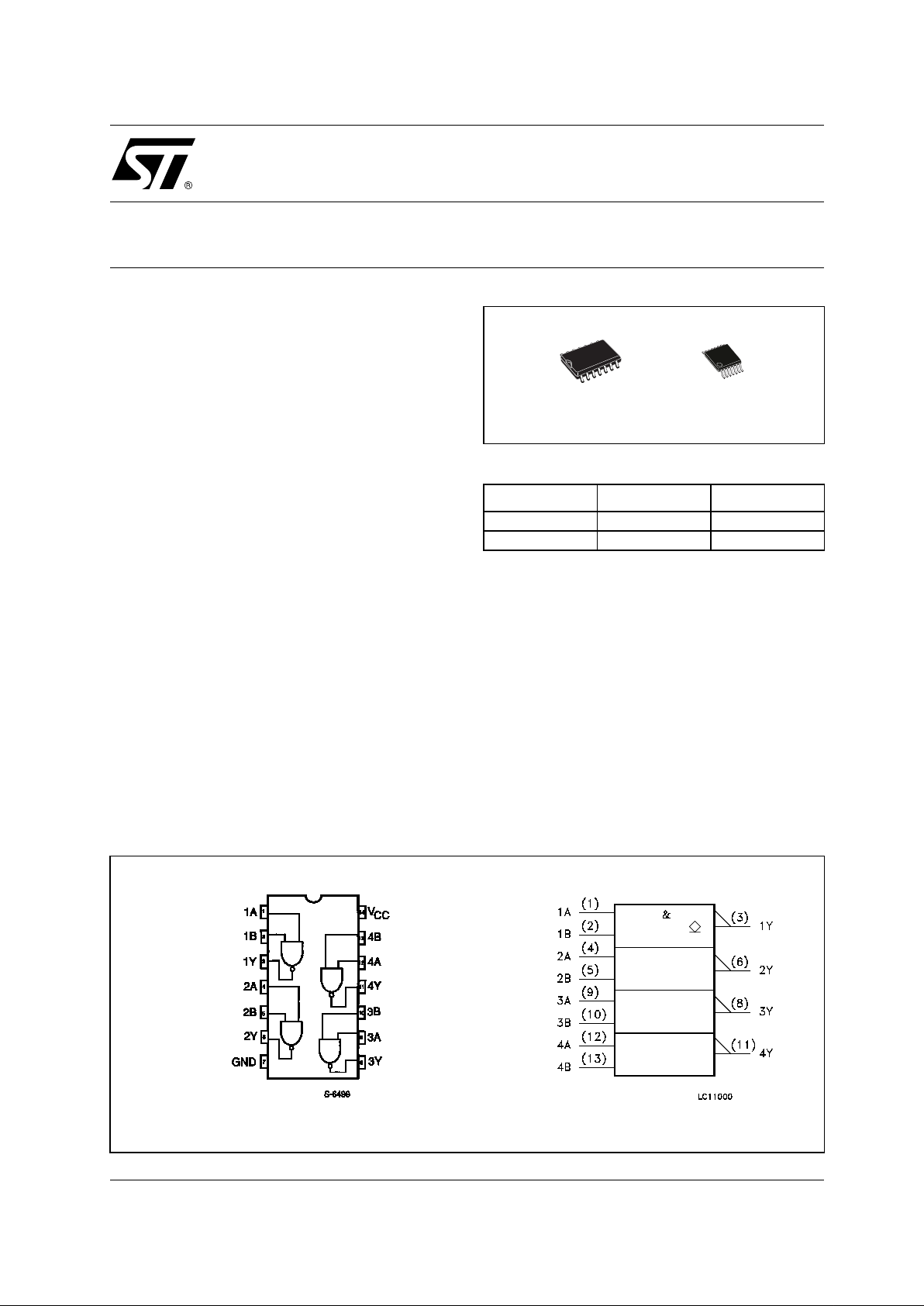
74VHC03
QUAD 2-INPUT OPEN DRAIN NAND GATE
PIN CONNECTION AND IEC LOGIC SYMBOLS
ORDER CODES
PACKAGE TUBE T & R
SOP 74VHC03M 74VHC03MTR
TSSOP 74VHC03TTR
TSSOPSOP
74VHC03
2/8
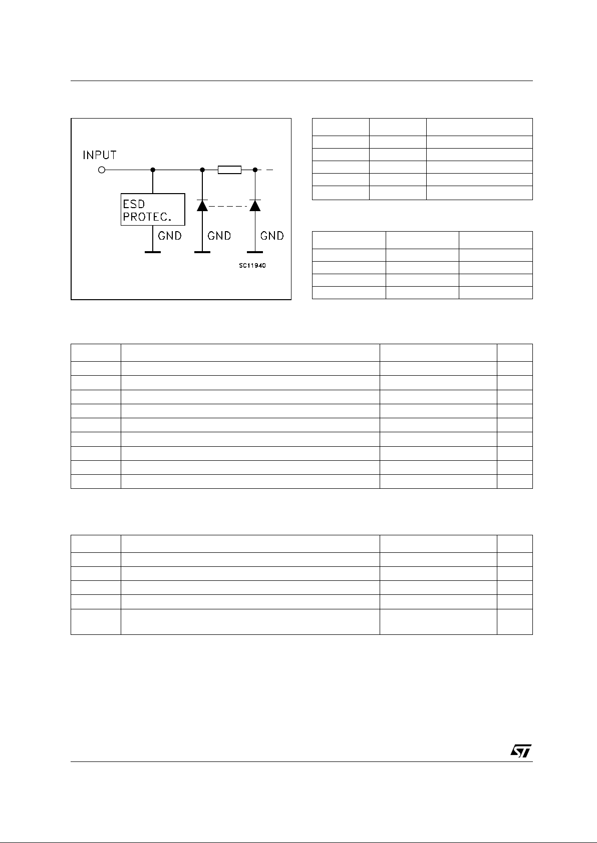
INPUT EQUIVALENT CIRCUIT PIN DESCRIPTION
TRUTH TABLE
Z: High Impedance
ABSOLUTE MAXIMUM RATINGS
Absolute Maximum Ratings are those values beyond which damage to the device may occur. Functional operation under these conditions is
not implied
RECOMMENDED OPERATING CONDITIONS
1) VIN from 30 % to 70% of V
CC
PIN No SYMBOL NAME AND FUNCTION
1, 4, 9, 12 1A to 4A Data Inputs
2, 5, 10, 13 1B to 4B Data Inputs
3, 6, 8, 11 1Y to 4Y Data Outputs
7 GND Ground (0V)
14
V
CC
Positive Supply Voltage
ABY
LLZ
LHZ
HLZ
HHL
Symbol Parameter Value Unit
V
CC
Supply Voltage
-0.5 to +7.0 V
V
I
DC Input Voltage
-0.5 to +7.0 V
V
O
DC Output Voltage -0.5 to VCC + 0.5
V
I
IK
DC Input Diode Current
- 20 mA
I
OK
DC Output Diode Current
± 20 mA
I
O
DC Output Current
± 25 mA
I
CC
or I
GND
DC VCC or Ground Current
± 50 mA
T
stg
Storage Temperature
-65 to +150 °C
T
L
Lead Temperature (10 sec)
300 °C
Symbol Parameter Value Unit
V
CC
Supply Voltage
2 to 5.5 V
V
I
Input Voltage
0 to 5.5 V
V
O
Output Voltage 0 to V
CC
V
T
op
Operating Temperature
-55 to 125 °C
dt/dv
Input Rise and Fall Time (note 1) (V
CC
= 3.3 ± 0.3V)
(V
CC
= 5.0 ± 0.5V)
0 to 100
0 to 20
ns/V
74VHC03
3/8
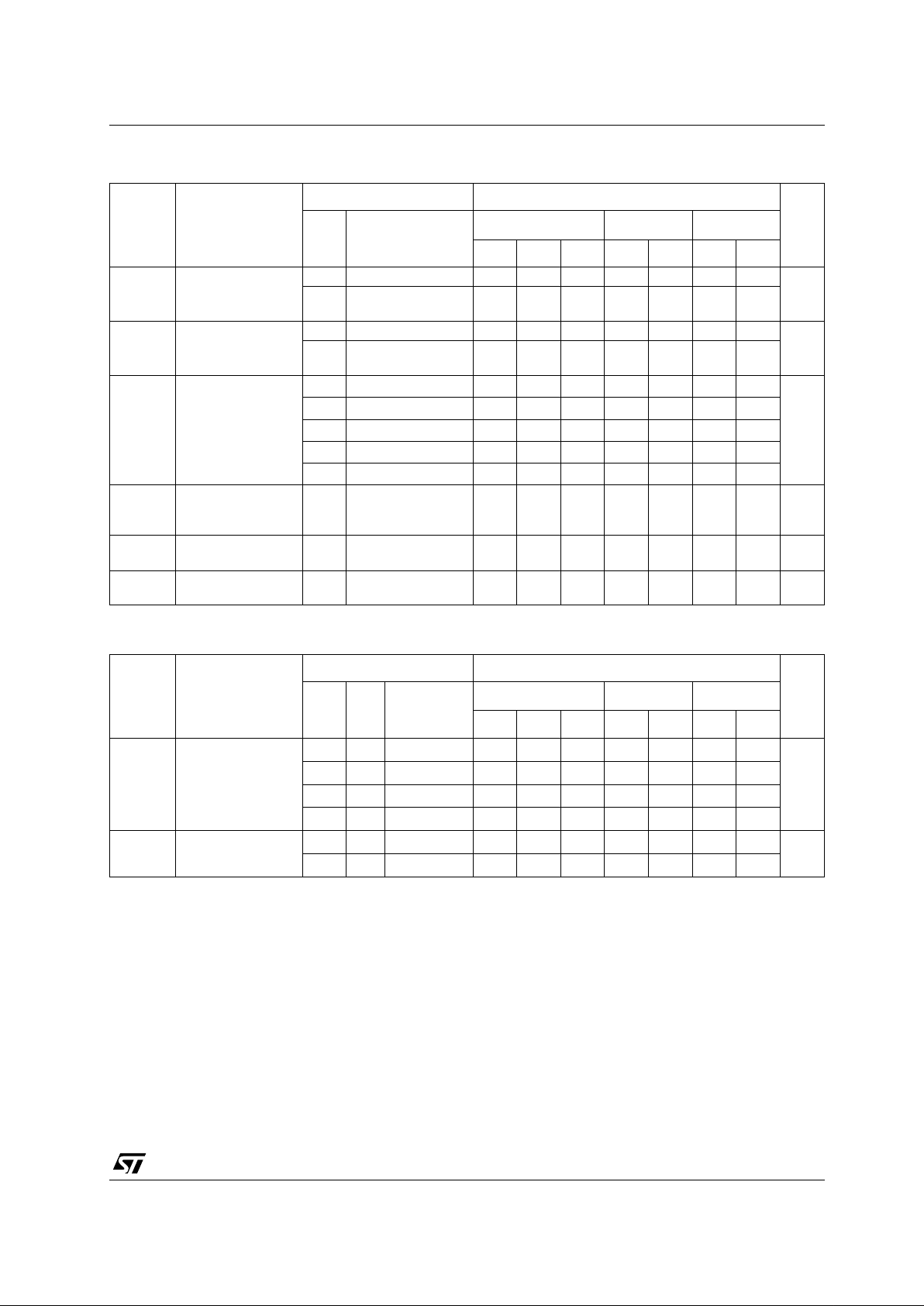
DC SPECIFICATIONS
AC ELECTRICAL CHARACTERISTICS (Input t
r
= tf = 3ns)
(*) Vol tage range is 3.3V ± 0.3V
(**) Voltage range is 5.0V ±
0.5V
Symbol Parameter
Test Condition Value
Unit
V
CC
(V)
T
A
= 25°C
-40 to 85°C -55 to 125°C
Min. Typ. Max. Min. Max. Min. Max.
V
IH
High Level Input
Voltage
2.0 1.5 1.5 1.5
V
3.0 to
5.5
0.7V
CC
0.7V
CC
0.7V
CC
V
IL
Low Level Input
Voltage
2.0 0.5 0.5 0.5
V
3.0 to
5.5
0.3V
CC
0.3V
CC
0.3V
CC
V
OL
Low Level Output
Voltage
2.0
I
O
=50 µA
0.0 0.1 0.1 0.1
V
3.0
I
O
=50 µA
0.0 0.1 0.1 0.1
4.5
I
O
=50 µA
0.0 0.1 0.1 0.1
3.0
I
O
=4 mA
0.36 0.44 0.55
4.5
I
O
=8 mA
0.36 0.44 0.55
I
OZ
High Impedance
Output Leakage
Current
5.5
V
I
= VIH or V
IL
VO = VCC or GND
±0.25 ± 2.5 ± 2.5 µA
I
I
Input Leakage
Current
0 to
5.5
V
I
= 5.5V or GND
± 0.1 ± 1 ± 1 µA
I
CC
Quiescent Supply
Current
5.5
V
I
= VCC or GND
22020µA
Symbol Parameter
Test Condition Value
Unit
V
CC
(V)
C
L
(pF)
T
A
= 25°C
-40 to 85°C -55 to 125°C
Min. Typ. Max. Min. Max. Min. Max.
t
PZL
Output Enable
Time
3.3
(*)
15
R
L
= 1 KΩ
5.5 7.9 1.0 9.5 1.0 9.5
ns
3.3
(*)
50
R
L
= 1 KΩ
8.0 11.4 1.0 13.0 1.0 13.0
5.0
(**)
15
R
L
= 1 KΩ
3.7 5.5 1.0 6.5 1.0 6.5
5.0
(**)
50
R
L
= 1 KΩ
5.2 7.5 1.0 8.5 1.0 8.5
t
PLZ
Output Disable
Time
3.3
(*)
50
R
L
= 1 KΩ
8.0 11.4 1.0 13.0 1.0 13.0
ns
5.0
(**)
50
R
L
= 1 KΩ
5.2 7.5 1.0 8.5 1.0 8.5
 Loading...