

1/9June 2003
■ HIGH SPEED:
t
PD
= 0.3ns (TYP.) at VCC=5V
t
PD
= 0.4ns (TYP.) at VCC=3.3V
■ LOW POWER DISSIPATION:
I
CC
=1µA(MAX.) at TA= 25°C
■ LOW "ON" RESISTANCE:
R
ON
=6.5Ω (TYP.) AT VCC=5VI
I/O
=1mA
R
ON
=8.5Ω(TYP.) AT VCC=3.3VI
I/O
=1mA
■ SINE WAVE DISTORTION:
0.04% AT V
CC
=3.3Vf=1KHz
■ WIDE OPERATING RANGE:
V
CC
(OPR) = 2V TO 5.5V
■ IMPROVED LATCH-UP IMMUNITY
DESCRIPTION
The 74V2G66 is an advanced high-speed CMOS
DUAL BILATERAL SWITCH fabricated in silicon
gate C
2
MOS technology. It achieves high speed
propagation delay and VERY LOW ON
resistances while maintaining true CMOS low
power consumption. This bilateral switch handles
rail to rail analog and digital signals that may vary
across the full power supply range (from GND to
V
CC
).
The C input is provided to control the switch and
it’s compatible with standard CMOS output; the
switch is ON (port I/O is connected to Port O/ I)
when the C input is held high and OFF (high
impedance state exists between the t w o ports)
when C is held low. It c an be used in m any
application as Batt ery Powered System, Test
Equipment. It’s available in the comm erc ial and
extended temperature range in SOT23-8L
package. All inputs and output are equipped with
protection circuits against s tatic discharge, giving
them ESD immunity and tra nsient excess voltage.
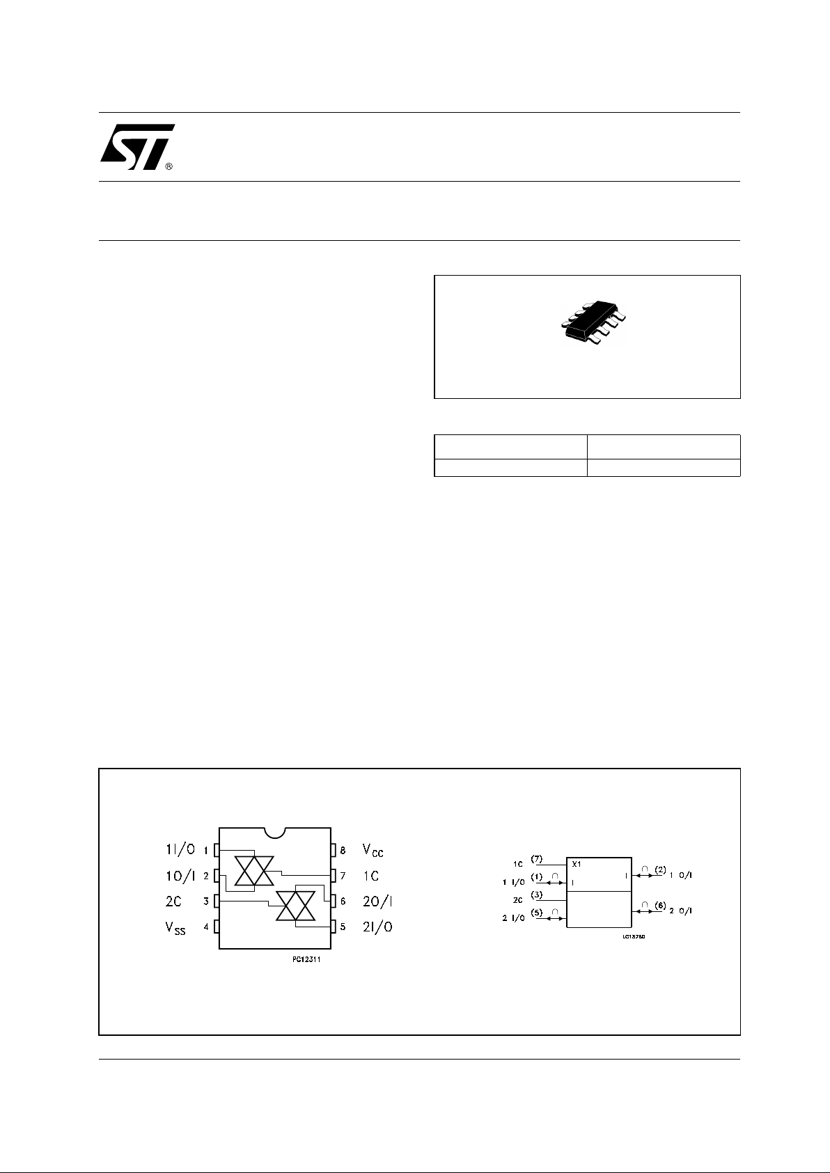
74V2G66
DUAL BILATERAL SWITCH
PIN CONNECTION AND IEC LOGIC SYMBOLS
ORDER CODES
PACKAGE T & R
SOT23-8L 74V2G66STR
SOT23-8L
74V2G66
2/9
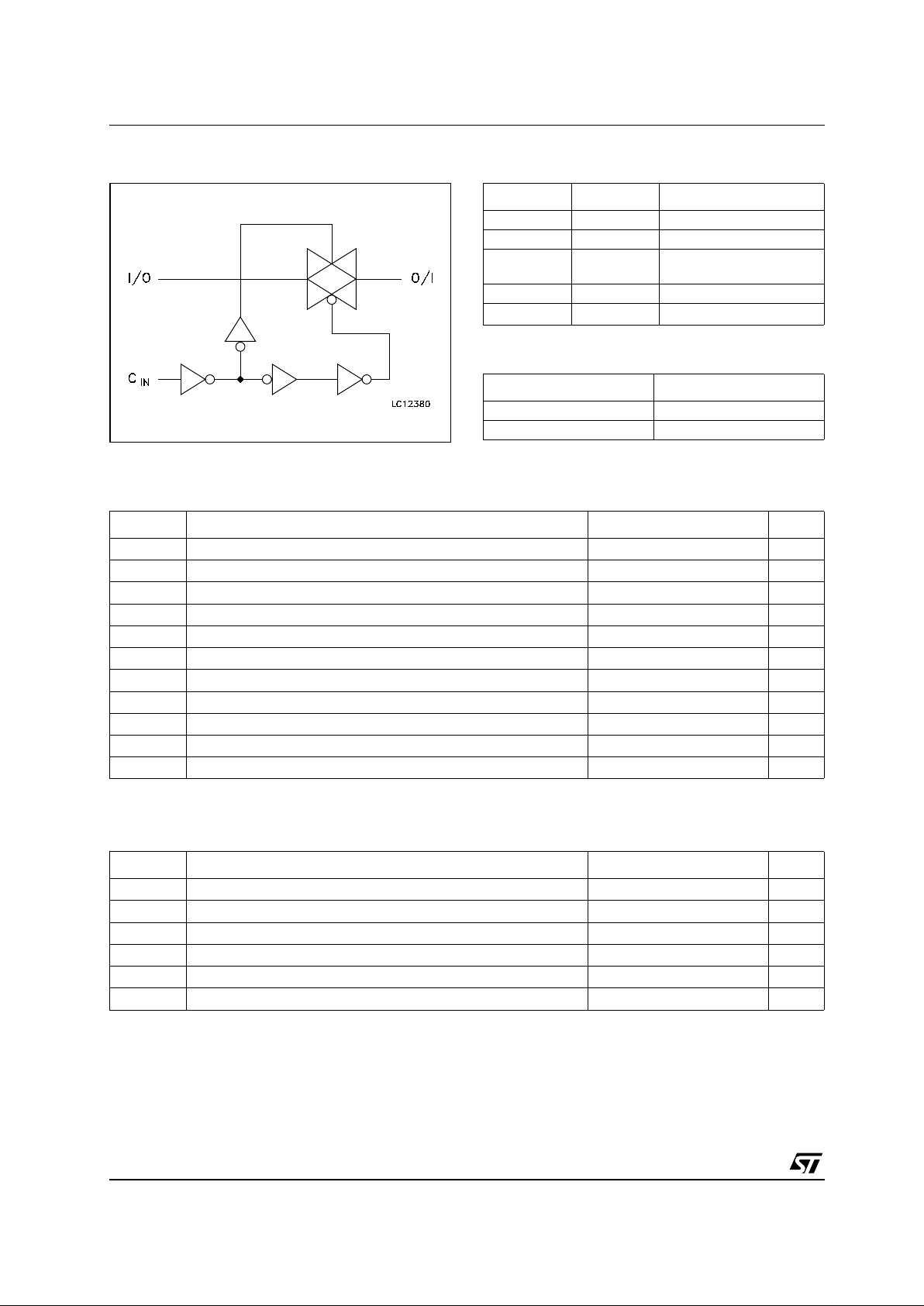
INPUT EQUIVALENT CIRCUIT PIN DESCRIPTION
TRUTH TABLE
* : High Impedance State
ABSOLUTE MAXIMUM RATINGS
Absolute Maximum Ratings are those values beyond which damage to the device may occur. Functional operation under these conditions is
not implied
RECOMMENDED OPERATING CONDITIONS
1) VINfrom30% to 70% of VCCon control pin
PIN No SYMBOL NAME AND FUNCTION
1, 5 1I/O, 2I/O Independent Input/Output
2, 6 1O/I, 2O/I Independent Output/Input
7, 3 1C, 2C
Enable Input (Active
HIGH)
4 GND Ground (0V)
8
V
CC
Positive Supply Voltage
CONTROL SWITCH FUNCTION
HON
L OFF *
Symbol Parameter Value Unit
V
CC
Supply Voltage
-0.5 to +7.0 V
V
I
DC Input Voltage -0.5 to VCC+ 0.5
V
V
IC
DC Control Input Voltage
-0.5 to +7.0 V
V
O
DC Output Voltage -0.5 to VCC+ 0.5
V
I
IK
DC Input Diode Current
± 20 mA
I
IK
DC Control Input Diode Current
-20 mA
I
OK
DC Output Diode Current
± 20 mA
I
O
DC Output Current
± 50 mA
I
CC
or I
GND
DC VCCor Ground Current
± 50 mA
T
stg
Storage Temperature
-65 to +150 °C
T
L
Lead Temperature (10 sec)
300 °C
Symbol Parameter Value Unit
V
CC
Supply Voltage
2 to 5.5 V
V
I
Input Voltage 0 to V
CC
V
V
IC
Control Input Voltage
0 to 5.5 V
V
O
Output Voltage 0 to V
CC
V
T
op
Operating Temperature
-55 to 125 °C
dt/dv
Input Rise and Fall Time (note 1) V
CC
= 5.0V
0 to 20 ns/V
74V2G66
3/9
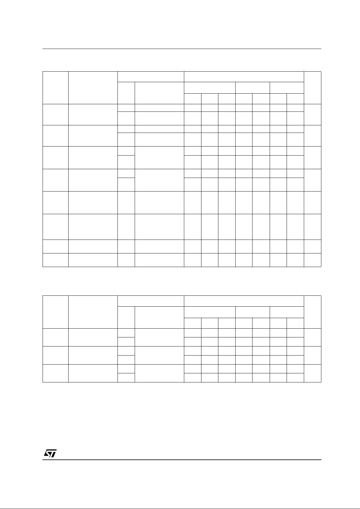
DC SPECIFICATIONS
(*) Voltage range is3.3V ± 0.3V
(**) Voltage range is 5V ± 0.5V
AC ELECTRICAL CHARACTERISTICS (CL= 50pF, Input tr=tf= 3ns)
(*) Voltage range is3.3V ± 0.3V
(**) Voltage range is 5.0V ± 0.5V
Symbol Parameter
Test Condition Value
Unit
V
CC
(V)
T
A
= 25°C
-40 to 85°C -55 to 125°C
Min. Typ. Max. Min. Max. Min. Max.
V
IH
High Level Input
Voltage
2.0 1.5 1.5 1.5
V
2.7to
5.5
0.7V
CC
0.7V
CC
0.7V
CC
V
IL
Low Level Input
Voltage
2.0 0.5 0.5 0.5
V
2.7to
5.5
0.3V
CC
0.3V
CC
0.3V
CC
R
ON
ON Resistance
3.3
(*)
VIC=V
IH
V
I/O=VCC
to GND
I
I/O
≤ 1mA
12.5 19 23 27
Ω
5.0
(**)
7.5 10 12 14
R
ON
ON Resistance
3.3
(*)
VIC=V
IH
V
I/O=VCC
or GND
I
I/O
≤ 1mA
8.5 10.5 12.5 15
Ω
5.0
(**)
6.5 8.5 10 12
I
OFF
Input/Output
Leakage Current
(SWITCH OFF)
5.5
V
OS=VCC
to GND
V
IS=VCC
to GND
V
IC=VIL
±0.1 ± 1 ± 5 µA
I
IZ
Switch Input
Leakage Current
(SWITCH ON,
OUTPUT OPEN)
5.5
V
OS=VCC
to GND
V
IC=VIH
±0.1 ± 1 ± 5 µA
I
IN
Control Input
Leakage Current
0to
5.5
V
IC
= 5.5V or GND
± 0.1 ± 1.0 ± 1.0 µA
I
CC
Quiescent Supply
Current
5.5
V
I=VCC
or GND
11020µA
Symbol Parameter
Test Condition Value
Unit
V
CC
(V)
T
A
= 25°C
-40 to 85°C -55 to 125°C
Min. Typ. Max. Min. Max. Min. Max.
t
PD
Delay Time
3.3
(*)
tr=tf=6ns
0.4 0.8 1.2 2.4
ns
5.0
(**)
0.3 0.6 1.0 2.0
t
PLZ
t
PHZ
Output Disable
Time
3.3
(*)
RL= 500 Ω
5.0 7.5 9.0 10.0
ns
5.0
(**)
5.0 7.5 9.0 10.0
t
PZL
t
PZH
Output Enable
Time
3.3
(*)
RL=1KΩ
2.5 4.0 5.0 7.0
ns
5.0
(**)
2.0 4.0 5.0 7.0
 Loading...