

1/8June 2003
■ HIGH SPEED: t
PD
= 3.0ns (TYP.) at VCC=5V
■ LOW POWER DISSIPATION:
I
CC
=1µA(MAX.) atTA=25°C
■ HIGH NOISE IMMUNITY:
V
NIH=VNIL
= 28% VCC(MIN.)
■ POWER DOWN PROTECTION ON INPUTS
AND OUTPUTS
■ SYMMETRICAL OUTPUT IMPEDANCE:
|I
OH
|=IOL=8mA(MIN)atVCC=4.5V
II
OH
|=IOL=4mA(MIN)atVCC=3.0V
■ BALANCED PROPAGATION DELAYS:
t
PLH
≅ t
PHL
■ OPERATING VOLTAGE RANG E:
V
CC
(OPR) = 2V to 5.5V
■ IMPROVED LATCH-UP IMMUNITY
DESCRIPTION
The 74V2G32 is an advanced high-speed CMOS
DUAL 2-INPUT OR GATE fabricated with
sub-micron silicon gate and double-layer metal
wiring C
2
MOS technology.
The internal circuit is composed of 3 st ages
including buffer output, w hich provide high noise
immunity and stable output.
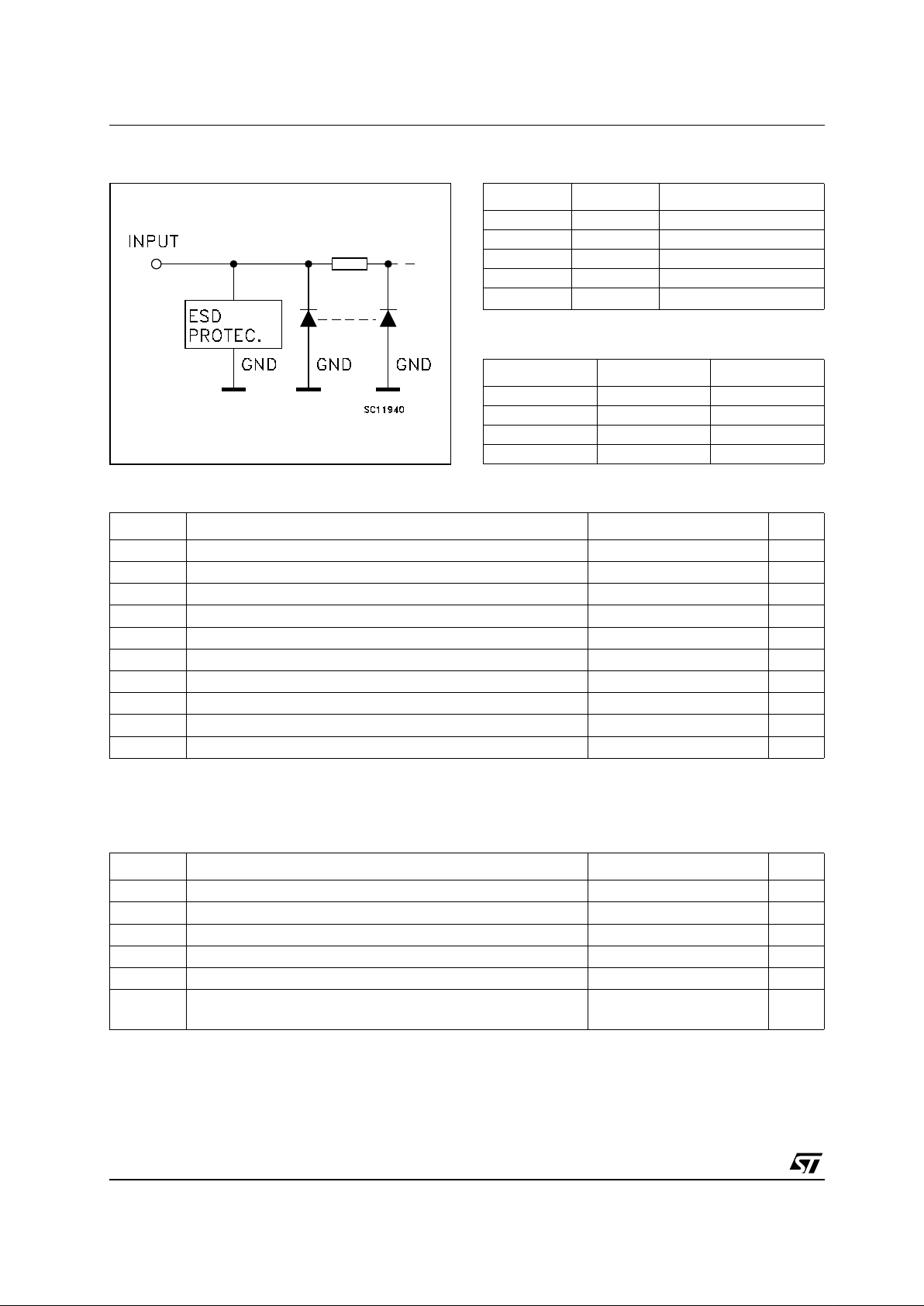
Power down protection is provided on all inputs
and outpu ts and 0 t o 7V can be accepted on
inputs with no regard to th e s upply voltage.
This device can be used to interface 5V to 3V
systems and it is ideal for portable applications
like personal digital assistant, camcorder and all
battery-powered equipment.
All inputs and outputs are equipped with
protection circuits aga inst st atic discharge, giving
them ESD immunity and transient excess voltage.
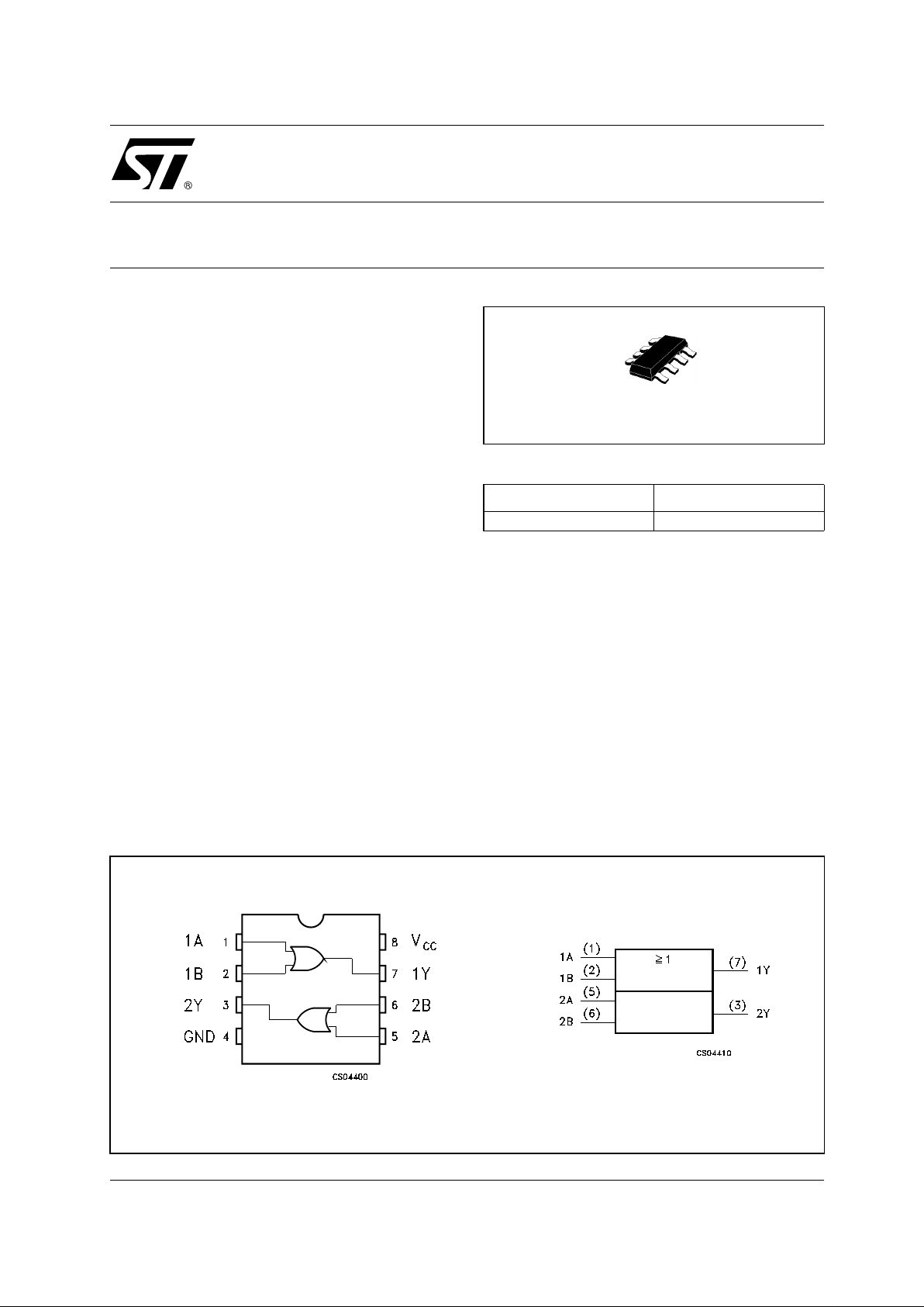
74V2G32
DUAL 2-INPUT OR GATE
PIN CONNECTION AND IEC LOGIC SYMBOLS
ORDER CODES
PACKAGE T & R
SOT23-8L 74V2G08STR
SOT23-8L
74V2G32
2/8
INPUT EQUIVALENT CIRCUIT PIN DESCRIPTION
TRUTH TABLE
ABSOLUTE MAXIMUM RATINGS
Absolute Maximum Ratings are those values beyond which damage to the device may occur. Functional operation under these conditions is
not implied.
1) VCC=0V
2) High or Low State
RECOMMENDED OPERATING CONDITIONS
1) VCC=0V
2) High or Low State
3) V
IN
from30%to70% ofV
CC
PIN No SYMBOL NAME QND FUNCTION
1, 5 1A, 2A Data Input
2, 6 1B, 2B Data Input
7, 3 1Y, 2Y Data Output
4 GND Ground (0V)
8
V
CC
Positive Supply Voltage
nA nB nY
LLL
LHH
HLH
HHH
Symbol Parameter Value Unit
V
CC
Supply Voltage
-0.5 to +7.0 V
V
I
DC Input Voltage
-0.5 to +7.0 V
V
O
DC Output Voltage (see note 1)
-0.5 to +7.0 V
V
O
DC Output Voltage (see note 2) -0.5 to VCC+ 0.5
V
I
IK
DC Input Diode Current
− 20 mA
I
OK
DC Output Diode Current
− 20 mA
I
O
DC Output Current
± 25 mA
I
CC
or I
GND
DC VCCor Ground Current
± 50 mA
T
stg
Storage Temperature
-65 to +150 °C
T
L
Lead Temperature (10 sec)
260 °C
Symbol Parameter Value Unit
V
CC
Supply Voltage
2 to 5.5 V
V
I
Input Voltage
0 to 5.5 V
V
O
Output Voltage (see note 1) 0 to 5.5
V
V
O
Output Voltage (see note 2) 0 to V
CC
V
T
op
Operating Temperature
-55 to 125 °C
dt/dv
Input Rise and Fall Time (note 3) (V
CC
=3.3±0.3V)
(V
CC
= 5.0 ± 0.5V)
0 to 100
0to20
ns/V
ns/V
74V2G32
3/8
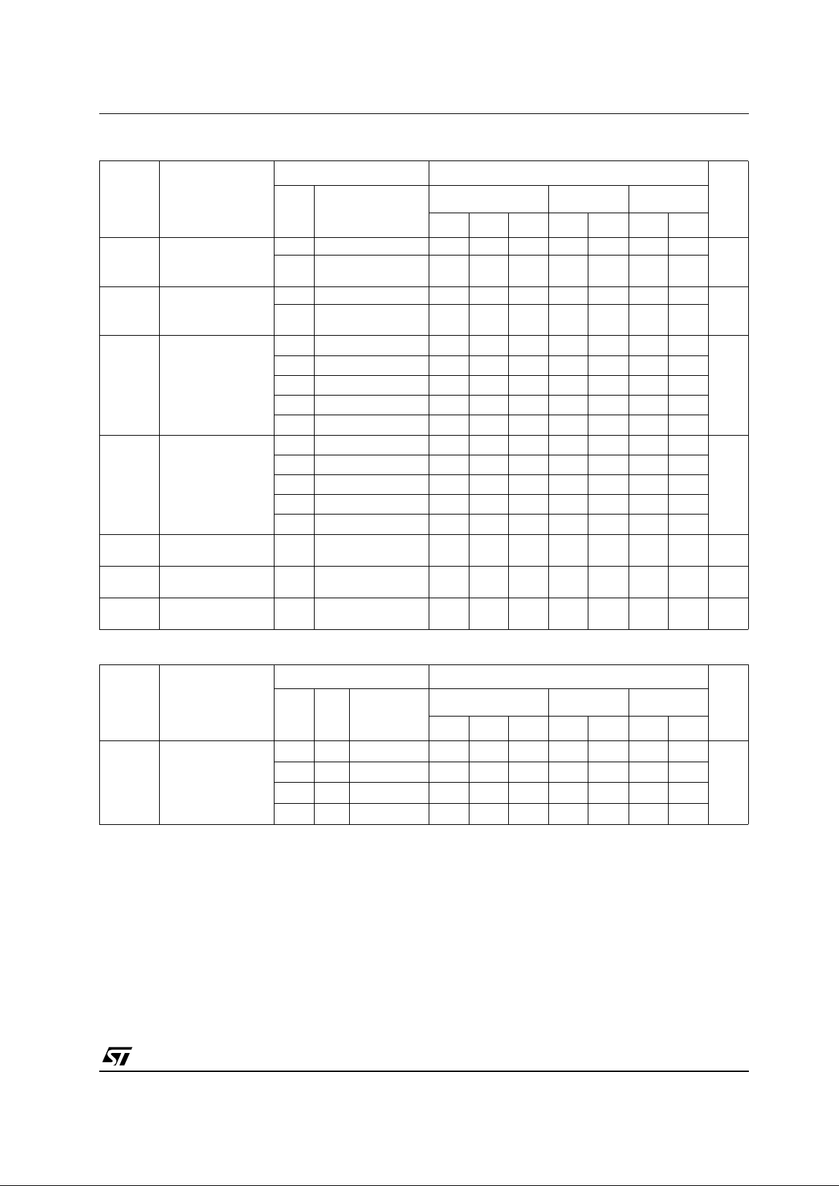
DC SPECIFICATIONS
AC ELECTRICAL CHARACTERISTICS (Input t
r=tf
=3ns)
(*) Voltage rangeis3.3V± 0.3V
(**) Voltage range is 5.0V ± 0.5V
Symbol Parameter
Test Condition Value
Unit
V
CC
(V)
T
A
= 25°C
-40 to 85°C -55 to 125°C
Min. Typ. Max. Min. Max. Min. Max.
V
IH
High Level Input
Voltage
2.0 1.5 1.5 1.5
V
3.0to
5.5
0.7V
CC
0.7V
CC
0.7V
CC
V
IL
Low Level Input
Voltage
2.0 0.5 0.5 0.5
V
3.0to
5.5
0.3V
CC
0.3V
CC
0.3V
CC
V
OH
High Level Output
Voltage
2.0
IO=-50 µA
1.9 2.0 1.9 1.9
V
3.0
I
O
=-50 µA
2.9 3.0 2.9 2.9
4.5
I
O
=-50 µA
4.4 4.5 4.4 4.4
3.0
I
O
=-4 mA
2.58 2.48 2.4
4.5
I
O
=-8 mA
3.94 3.8 3.7
V
OL
Low Level Output
Voltage
2.0
IO=50 µA
0.0 0.1 0.1 0.1
V
3.0
I
O
=50 µA
0.0 0.1 0.1 0.1
4.5
I
O
=50 µA
0.0 0.1 0.1 0.1
3.0
I
O
=4 mA
0.36 0.44 0.55
4.5
I
O
=8 mA
0.36 0.44 0.55
I
I
Input Leakage
Current
0to
5.5
VI= 5.5V or GND
± 0.1 ± 1 ± 1 µA
I
CC
Quiescent Supply
Current
5.5
V
I=VCC
or GND
11020µA
I
OPD
Power down Output
Leakage Current
0
V
O
= 5.5
0.5 5 10 µA
Symbol Parameter
Test Condition Value
Unit
V
CC
(V)
C
L
(pF)
T
A
= 25°C
-40 to 85°C -55 to 125°C
Min. Typ. Max. Min. Max. Min. Max.
t
PLHtPHL
Propagation Delay
Time
3.3
(*)
15 3.7 7.0 1.0 8.0 1.0 9.0
ns
3.3
(*)
50 5.3 8.0 1.0 9.5 1.0 10.5
5.0
(**)
15 3.0 5.0 1.0 6.0 1.0 7.0
5.0
(**)
50 4.1 6.5 1.0 7.5 1.0 8.5

74V2G32
4/8
CAPACITANCE CHARACTERISTICS
1) CPDis defined as the value of the IC’s internal equivalent capacitance which is calculated from the operating current consumption without
load. (Refer to Test Circuit). Average current can be obtained by the following equation. I
CC(opr)=CPDxVCCxfIN+ICC
/2
DYNAMIC SWITCHING CHARACTERISTICS
1) Number of output defined as "n". Measured with "n-1" outputs switching from HIGH to LOW or LOW to HIGH. The remaining outputs is
measured in the LOW state.
Symbol Parameter
Test Condition Value
Unit
T
A
= 25°C
-40 to 85°C -55 to 125°C
Min. Typ. Max. Min. Max. Min. Max.
C
IN
Input Capacitance
410 10 10pF
C
PD
Power Dissipation
Capacitance
(note 1)
12 pF
Symbol Parameter
Test Condition Value
Unit
V
CC
(V)
T
A
=25°C
Min. Max.
V
OLP
Dynamic Low Level Quiet Output (note 1)
5.0
C
L
=50pF
V
IL
=0V,VIH= 3.3V
0.8
V
V
OLV
-0.8

74V2G32
5/8
TEST CIRCUIT
CL= 15/50pF or equivalent (includes jig and probe capacitance)
R
T=ZOUT
of pulse generator (typically 50Ω)
WAVEFORM: PROPAGATION DELAY (f=1MHz; 50% duty cycle)

74V2G32
6/8
DIM.
mm. mils
MIN. TYP MAX. MIN. TYP. MAX.
A 0.90 1.45 35.4 57.1
A1 0.00 0.15 0.0 5.9
A2 0.90 1.30 35.4 51.2
b 0.22 0.38 8.6 14.9
C 0.09 0.20 3.5 7.8
D 2.80 3.00 110.2 118.1
E 2.60 3.00 102.3 118.1
E1 1.50 1.75 59.0 68.8
e0.65 25.6
e1 1.95 76.7
L 0.35 0.55 13.7 21.6
SOT23-8L MECHANICAL DATA

74V2G32
7/8
DIM.
mm. inch
MIN. TYP MAX. MIN. TYP. MAX.
A 180 7.086
C 12.8 13.0 13.2 0.504 0.512 0.519
D 20.2 0.795
N 60 2.362
T 14.4 0.567
Ao 3.13 3.23 3.33 0.123 0.127 0.131
Bo 3.07 3.17 3.27 0.120 0.124 0.128
Ko 1.27 1.37 1.47 0.050 0.054 0.0.58
Po 3.9 4.0 4.1 0.153 0.157 0.161
P 3.9 4.0 4.1 0.153 0.157 0.161
Tape & Reel SOT23-xL MECHANICAL DATA

74V2G32
8/8
Information furnished is believed to be accurate and reliable. However, STMicroelectronics assumes no responsibility for the
consequences of use o f suc h inf ormat ion n or f or an y infr ingeme nt of paten ts or oth er ri gh ts of third part ies whic h may resul t f rom
its use. No license is granted by implication or otherwise under any patent or patent rights of STMicroelectronics. Specifications
mentioned in this publication are subject to change without notice. This publication supersedes and replaces all information
previously supplied. STMicroelectronics products are not authorized for use as critical components in life support devices or
systems without express written approval of STMicroelectronics.
© The ST logo is a registered trademark of STMicroelectronics
© 2003 STMicroelectronics - Printed in Italy - All Rights Reserved
STMicroelectronics GROUP OF COMPANIES
Australia - Brazil - Canada - China - Finland - France - Germany - Hong Kong - India - Israel - Italy - Japan - Malaysia - Malta - Morocco
Singapore - Spain - Sweden - Switzerland - United Kingdom - United States.
© http://www.st.com
 Loading...