

1/7June 2003
■ HIGH SPEED: t
PD
= 3.9ns (TYP.) at VCC=5V
■ LOW POWER DISSIPATION:
I
CC
=1µA(MAX.) atTA=25°C
■ HIGH NOISE IMMUNITY:
V
NIH=VNIL
= 28% VCC(MIN.)
■ POWER DOWN PROTECTION ON INPUTS
■ OPERATING VOLTAGE RANGE:
V
CC
(OPR) = 2V to 5.5V
■ IMPROVED LATCH-UP IMMUNITY
DESCRIPTION
The 74V2G03 is an advanced high-speed CMOS
DUAL 2-INPUT OPEN DRAIN NAND GA TE
fabricated with sub-micron silicon gate and
double-layer metal wiring C
2
MOS technology.
The internal circuit is composed of 3 stages
including buffer output, which provide high noise
immunity and stable output.
The device can, with an external pull-up resistor,
be used in wired AND configuration. This device
can also be used as a led driver in any other
application requiring current sink.
Power down protection is provide d on all inputs
and 0 to 7V can be accept ed on inputs with no
regard to the supply voltage. This device can be
usedto interface 5V to 3V.
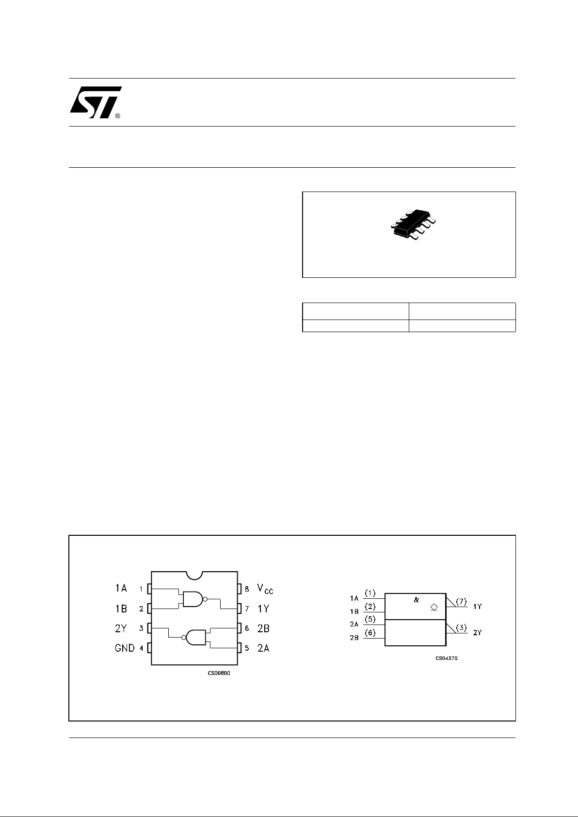
74V2G03
DUAL 2-INPUT OPEN DRAIN NAND GATE
PIN CONNECTION AND IEC LOGIC SYMBOLS
ORDER CODES
PACKAGE T & R
SOT23-8L 74V2G03STR
SOT23-8L
74V2G03
2/7
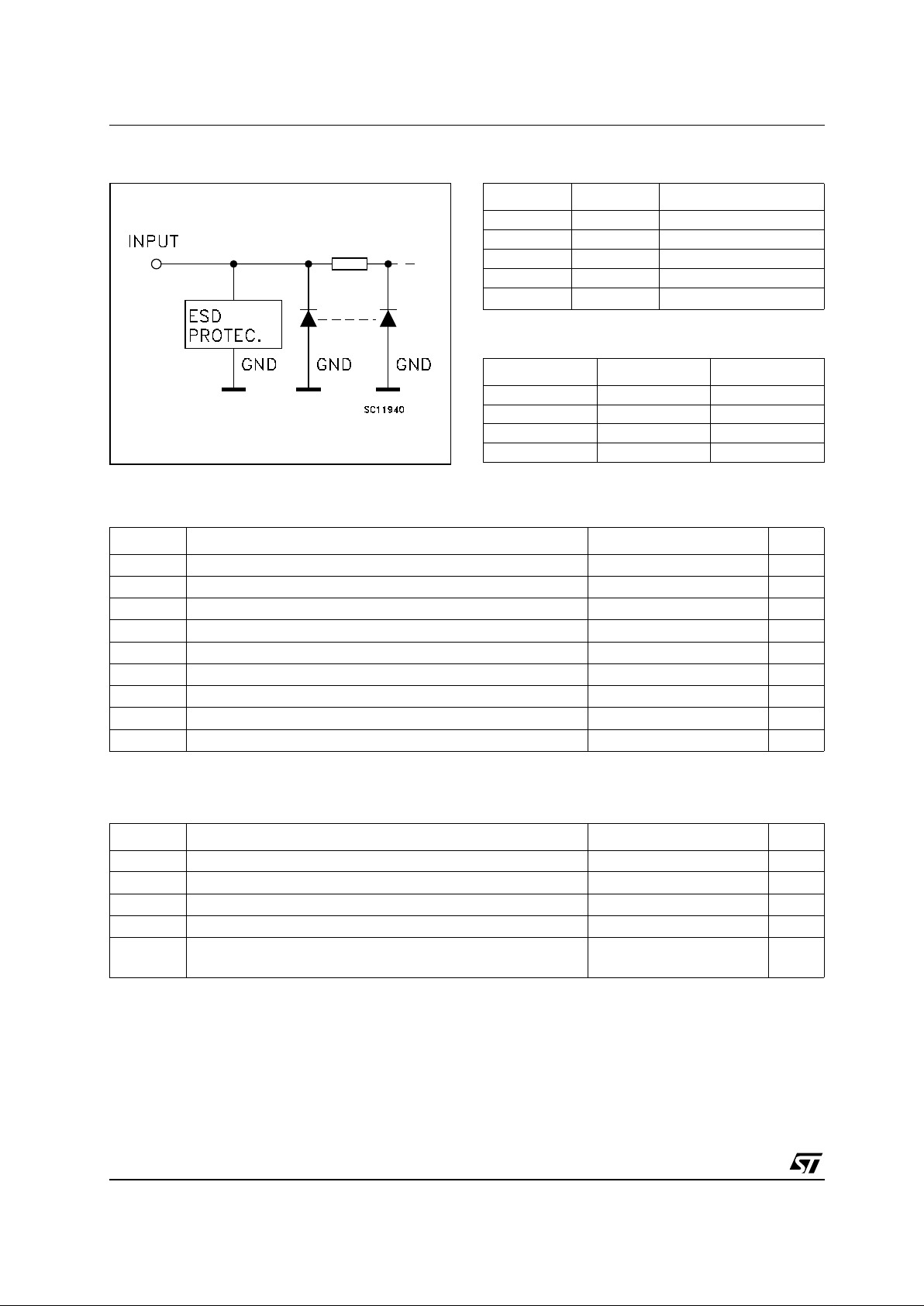
INPUT EQUIVALENT CIRCUIT PIN DESCRIPTION
TRUTH TABLE
Z: HighImpedance
ABSOLUTE MAXIMUM RATINGS
Absolute Maximum Ratings are those values beyond which damage to the device may occur. Functional operation under these conditions is
not implied.
RECOMMENDED OPERATING CONDITIONS
1) VINfrom30% to 70% of V
CC
PIN N° SYMBOL NAME QND FUNCTION
1, 5 1A, 2A Data Input
2, 6 1B, 2B Data Input
7, 3 1Y, 2Y Data Output
4 GND Ground (0V)
8
V
CC
Positive Supply Voltage
ABY
LLZ
LHZ
HLZ
HHL
Symbol Parameter Value Unit
V
CC
Supply Voltage
-0.5 to +7.0 V
V
I
DC Input Voltage
-0.5 to +7.0 V
V
O
DC Output Voltage -0.5 to VCC+ 0.5
V
I
IK
DC Input Diode Current
-20 mA
I
OK
DC Output Diode Current
± 20 mA
I
O
DC Output Current
± 25 mA
I
CC
or I
GND
DC VCCor Ground Current
± 50 mA
T
stg
Storage Temperature
-65 to +150 °C
T
L
Lead Temperature (10 sec)
260 °C
Symbol Parameter Value Unit
V
CC
Supply Voltage
2 to 5.5 V
V
I
Input Voltage
0 to 5.5 V
V
O
Output Voltage 0 to V
CC
V
T
op
Operating Temperature
-55 to 125 °C
dt/dv
Input Rise and Fall Time (note 1) (V
CC
=3.3±0.3V)
(V
CC
= 5.0 ± 0.5V)
0 to 100
0to20
ns/V
ns/V
74V2G03
3/7
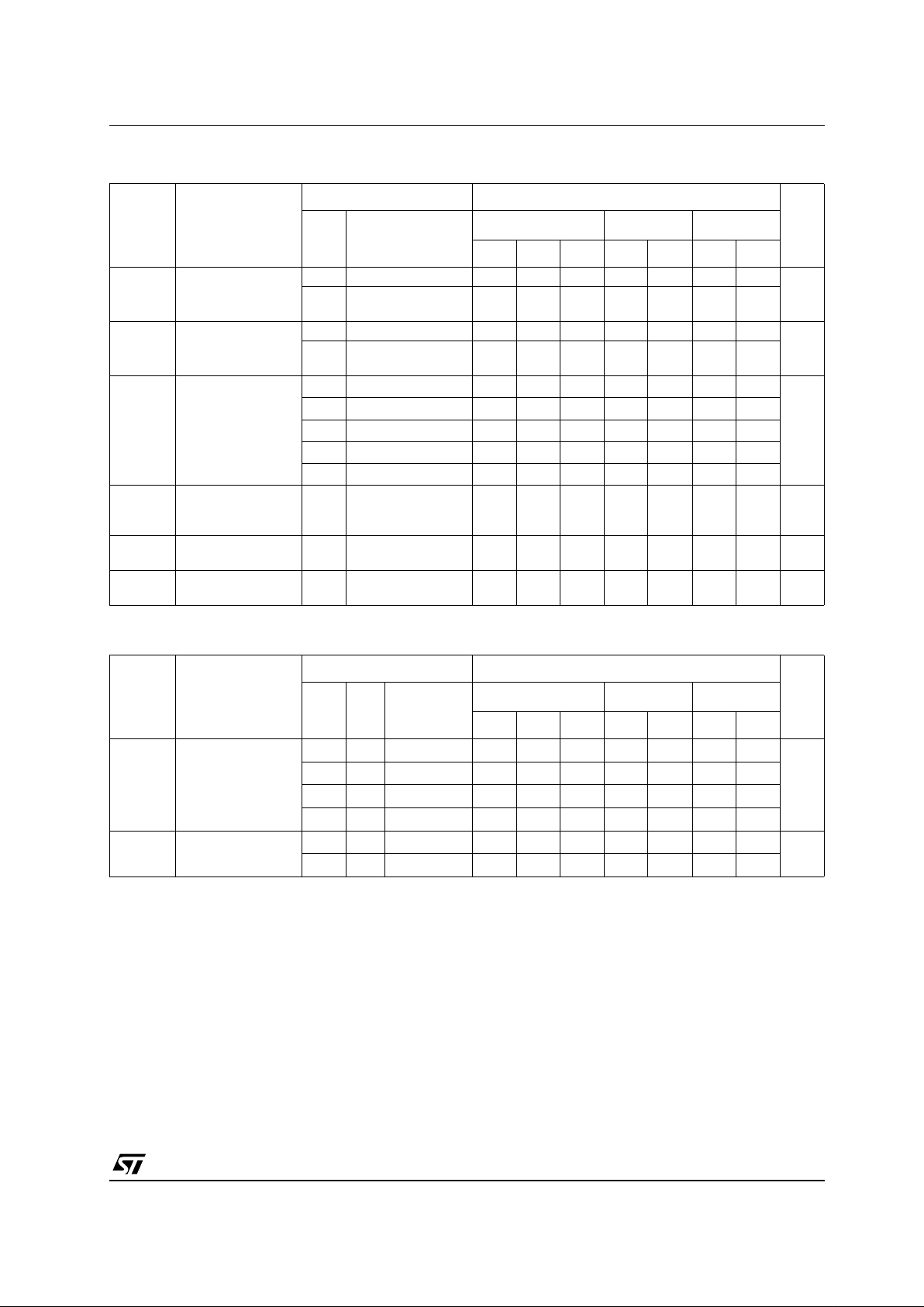
DC SPECIFICATIONS
AC ELECTRICAL CHARACTERISTICS
(*) Voltage range is3.3V ± 0.3V
(**) Voltage range is 5.0V ± 0.5V
Symbol Parameter
Test Condition Value
Unit
V
CC
(V)
T
A
= 25°C
-40 to 85°C -55 to 125°C
Min. Typ. Max. Min. Max. Min. Max.
V
IH
High Level Input
Voltage
2.0 1.5 1.5 1.5
V
3.0to
5.5
0.7V
CC
0.7V
CC
0.7V
CC
V
IL
Low Level Input
Voltage
2.0 0.5 0.5 0.5
V
3.0to
5.5
0.3V
CC
0.3V
CC
0.3V
CC
V
OL
Low Level Output
Voltage
2.0
IO=50 µA
0.0 0.1 0.1 0.1
V
3.0
I
O
=50 µA
0.0 0.1 0.1 0.1
4.5
I
O
=50 µA
0.0 0.1 0.1 0.1
3.0
I
O
=4 mA
0.36 0.44 0.55
4.5
I
O
=8 mA
0.36 0.44 0.55
I
OZ
High Impedance
Output Leakage
Current
5.5
V
I=VIH
or V
IL
VO=VCCor GND
±
0.25
± 2.5 ± 5 µA
I
I
Input Leakage
Current
0to
5.5
V
I
= 5.5V or GND
± 0.1 ± 1 ± 1 µA
I
CC
Quiescent Supply
Current
5.5
V
I=VCC
or GND
11020µA
Symbol Parameter
Test Condition Value
Unit
V
CC
(V)
C
L
(pF)
T
A
= 25°C
-40 to 85°C -55 to 125°C
Min. Typ. Max. Min. Max. Min. Max.
t
PZL
Propagation Delay
Time
3.3
(*)
15 4.8 6.5 1.0 8.0 1.0 9.0
ns
3.3
(*)
50 5.3 7.5 1.0 9.0 1.0 10.0
5.0
(**)
15 3.9 5.5 1.0 6.5 1.0 7.5
5.0
(**)
50 4.3 6.0 1.0 7.5 1.0 8.5
t
PLZ
Propagation Delay
Time
3.3
(*)
50 6.8 9.5 1.0 10.0 1.0 11.0
ns
5.0
(**)
50 4.8 6.5 1.0 7.0 1.0 8.0
 Loading...