

SGS Thomson Microelectronics 74V1T79STR, 74V1T79CTR Datasheet
1/9July 2001
■ HIGH SPEED:
f
MAX
= 180MHz (TYP.) at VCC = 5V
t
CK-Q
= 3.9ns (TYP.) at VCC = 5V
■ LOW POWER DISSIPATION:
I
CC
= 1µA(MAX.) at TA=25°C
■ COMPATIBLE WITH TTL OUTPUTS:
V
IH
= 2V (MIN), VIL = 0.8V (MAX)
■ POWER DOWN PROTECTION ON INPUT S
■ SYMMETRICAL OUTPUT IMPEDANCE:
|I
OH
| = IOL = 8mA (MIN) at VCC = 4.5V
■ BALANCED PROPAGATION DELAYS:
t
PLH
≅ t
PHL
■ OPERATING VOL TAGE RANGE:
V
CC
(OPR) = 4.5V to 5.5V
■ IMPROVED LATCH-UP IMMUNITY
DESCRIPTION
The 74V1T79 is an advanc ed high-speed CM OS
SINGLE POSITIVE EDGE TRIGGERED D-TYPE
FLIP-FLOP fabricated with sub-micron silicon
gate and double-layer metal wiring C
2
MOS
technology. It is designed to operate from 4.5V to
5.5V, making this device ideal for portable
applications.
This D-Type flip-flop is controlled by a clock input
(CK). On the positive transition of the clock, the Q
output will be set to the logic state t hat wa s s etup
at th e D input.
Following the hold time interval, data at the D input
can be changed without affecting the level at the
output. Power down protection is provided on
inputs and 0 to 7V can be accepted on inputs with
no regard to t he supply voltage. This device can
be used to interface 5V to 3V systems.
It’s available in the commercial and extended
temperature range.
All inputs and output are equippe d with prot ection
circuits against stati c disc harge , giving t hem ES D
immunity and transient excess voltage.
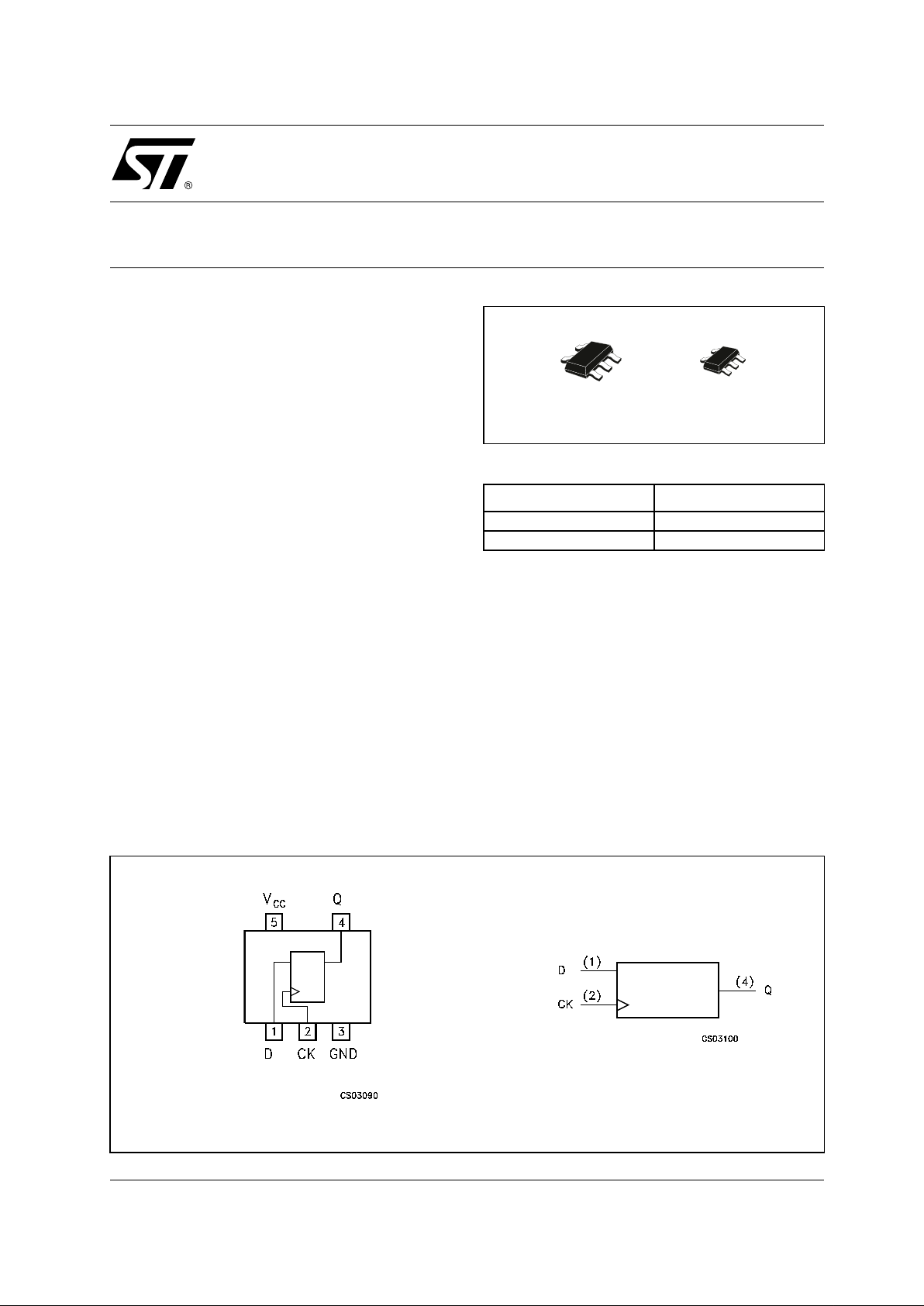
74V1T79
SINGLE POSITIVE EDGE TRIGGERED
D-TYPE FLIP-FLOP
PIN CONNECTION AND IEC LOGIC SYMBOLS
ORDER CODES
PACKAGE T & R
SOT23-5L 74V1T79STR
SOT323-5L 74V1T79CTR
SOT323-5LSOT23-5L
74V1T79
2/9
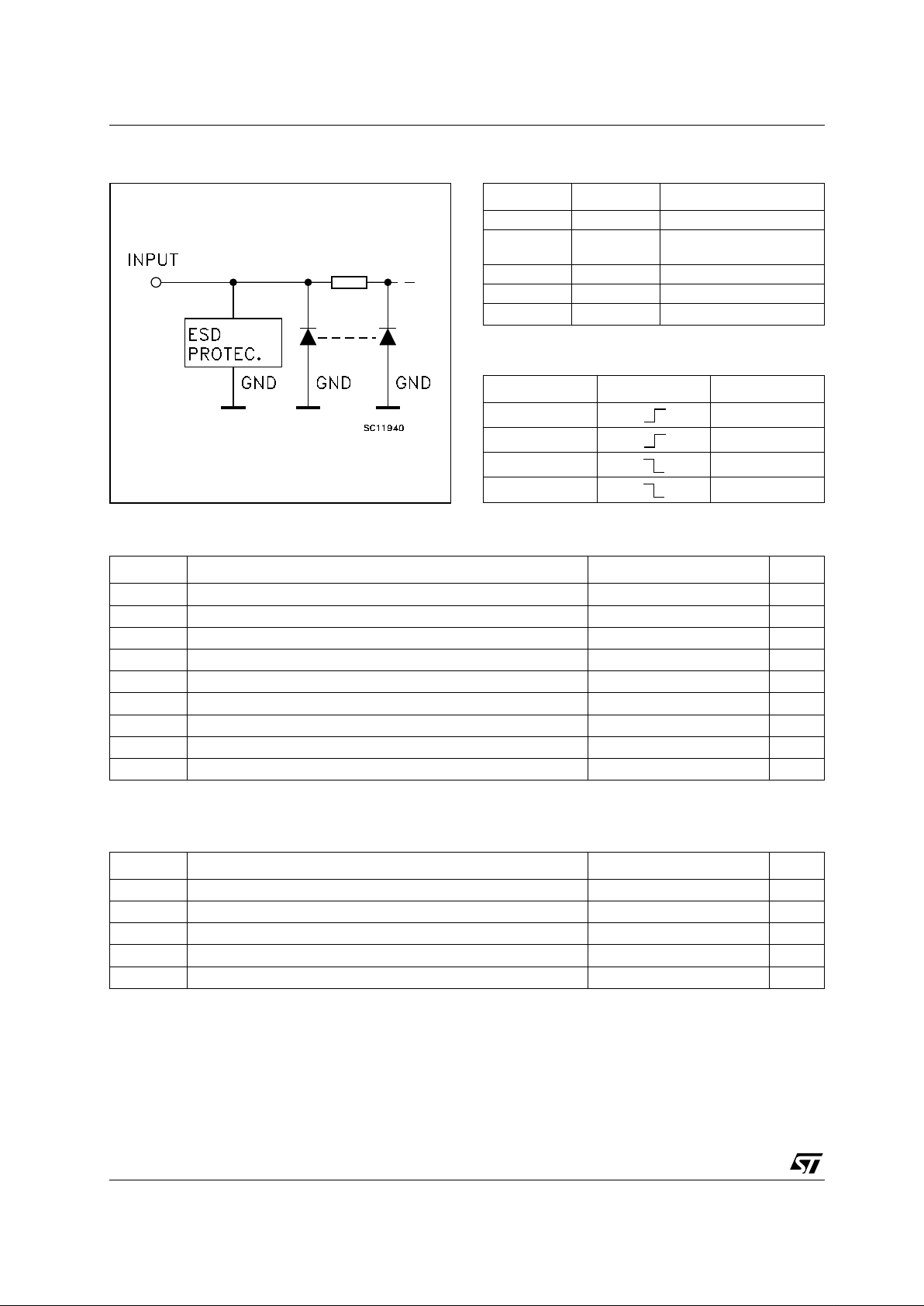
INPUT EQUIVALENT CIRCUIT PIN DESCRIPTION
TRUTH TABLE
ABSOLUTE MAXIMUM RATINGS
Absolute Maximum Ratings are those values beyond which damage to the device may occur. Functional operation under these conditions is
not implied
RECOMMENDED OPERATING CONDITIONS
1) VIN from 0.8V to 2V
PIN No SYMBOL NAME AND FUNCTION
1 D Data Input
2CK
Clock Input (Positive
Edge)
4 Q Flip-Flop Output
3 GND Ground (0V)
5
V
CC
Positive Supply Voltage
DCKQ
LL
HH
LQn
HQn
Symbol Parameter Value Unit
V
CC
Supply Voltage
-0.5 to +7.0 V
V
I
DC Input Voltage
-0.5 to +7.0 V
V
O
DC Output Voltage -0.5 to VCC + 0.5
V
I
IK
DC Input Diode Current
- 20 mA
I
OK
DC Output Diode Current
± 20 mA
I
O
DC Output Current
± 25 mA
I
CC
or I
GND
DC VCC or Ground Current
± 50 mA
T
stg
Storage Temperature
-65 to +150 °C
T
L
Lead Temperature (10 sec)
300 °C
Symbol Parameter Value Unit
V
CC
Supply Voltage
4.5 to 5.5 V
V
I
Input Voltage
0 to 5.5 V
V
O
Output Voltage 0 to V
CC
V
T
op
Operating Temperature
-55 to 125 °C
dt/dv
Input Rise and Fall Time (note 1) (V
CC
= 5.0 ± 0.5V)
0 to 20 ns/V
74V1T79
3/9
DC SPECIFICATIONS
AC ELECTRICAL CHARACTERISTICS (Input t
r
= tf = 3ns)
(*) Vol tage range is 5.0V ± 0.5V
CAPACITIVE CHARACTERISTICS
1) CPD is defined as the value of the IC’s internal equivalent capacitance which is calculated from the operating current consumption without
load. (R ef er to Test Circuit). Average operating current can be obtained by t he following equation. I
CC(opr)
= CPD x VCC x fIN + I
CC
Symbol Parameter
Test Condition Value
Unit
V
CC
(V)
T
A
= 25°C
-40 to 85°C -55 to 125°C
Min. Typ. Max. Min. Max. Min. Max.
V
IH
High Level Input
Voltage
4.5 to
5.5
222V
V
IL
Low Level Input
Voltage
4.5 to
5.5
0.8 0.8 0.8 V
V
OH
High Level Output
Voltage
4.5
IO=-50 µA 4.4 4.5 4.4 4.4 V
4.5
I
O
=-8 mA 3.94 3.8 3.7
V
OL
Low Level Output
Voltage
4.5
IO=50 µA 0.0 0.1 0.1 0.1 V
4.5
I
O
=8 mA 0.36 0.44 0.55
I
I
Input Leakage
Current
0 to
5.5
V
I
= 5.5V or GND
± 0.1 ± 1.0 ± 1.0 µA
I
CC
Quiescent Supply
Current
5.5
V
I
= VCC or GND
11020µA
I
CC
Additional Worst
Case Supply
Current
5.5
One Input at 3.4V,
other input at V
CC
or GND
1.35 1.5 1.5 mA
Symbol Parameter
Test Condition Value
Unit
V
CC
(V)
C
L
(pF)
T
A
= 25°C
-40 to 85°C -55 to 125°C
Min. Typ. Max. Min. Max. Min. Max.
t
PLH tPHL
Propagation Delay
Time CK to Q
5.0 (*) 15 3.9 5.5 1.0 6.5 1.0 7.5 ns
5.0 (*) 50 4.5 6.5 1.0 7.5 1.0 8.5
t
W
CK Pulse Width,
HIGH or LOW
5.0 (*) 3.0 3.0 3.0 ns
t
s
Setup Time D to
CK, HIGH or LOW
5.0 (*) 2.0 2.0 2.0 ns
t
h
Hold Time D to CK,
HIGH or LOW
5.0 (*) 1.0 1.0 1.0 ns
f
MAX
Maximum Clock
Frequency
5.0 (*) 50 120 180 120 120 MHz
Symbol Parameter
Test Condition Value
Unit
T
A
= 25°C
-40 to 85°C -55 to 125°C
Min. Typ. Max. Min. Max. Min. Max.
C
IN
Input Capacitance
4101010pF
C
PD
Power Dissipation
Capacitance
(note 1)
8pF
 Loading...