

1/11July 2001
■ HIGH SPEED:
t
PD
= 0.3ns (TYP.) at VCC = 5V
■ LOW POWER DISSIPATION:
I
CC
= 1µA(MAX.) at TA=25°C
■ LOW "ON" RESISTANCE:
R
ON
= 6.5Ω (TYP.) AT VCC = 5V I
I/O
= 1mA
■ SINE WAVE DISTORTION:
0.04% AT V
CC
= 5V f = 1KHz
■ COMPATIBLE WI TH TTL OUTPUTS ON
CONTROL PIN:
V
IH
= 2V (MIN), VIL = 0.8V (MAX)
■ OPERATING VOLTAG E RAN GE:
V
CC
(OPR) = 4.5V to 5.5V
■ IMPROVED LATCH-UP IMMUNITY
DESCRIPTION
The 74V1T66 is an advanc ed high-speed CM OS
SINGLE BILATERAL SWITCH fabricated in
silicon gate C
2
MOS technology. It achieves hi gh
speed propagation delay and VERY LOW ON
resistances while maintaining true CMOS low
power consumption. This bilateral switch handles
rail to rail analog and digital signal s that m ay v ary
across the full power supply range (from GND to
V
CC
).
The C input is provided to cont rol the switch a nd
it’s compatible with standard TTL output; the
switch is ON (port I/O is connected to Port O/I)
when the C input is held high and OFF (high
impedance state exists between the two ports)
when C is held low. It can be used in many
application as Battery Powered System, Test
Equipment. It’s available in the commercial and
extended temperature range in SOT23-5L and
SC-70-5L package.
All inputs and output are equippe d with prot ection
circuits against stati c disc harge , giving t hem ES D
immunity and transient excess voltage.
74V1T66
SINGLE BILATERAL SWITCH
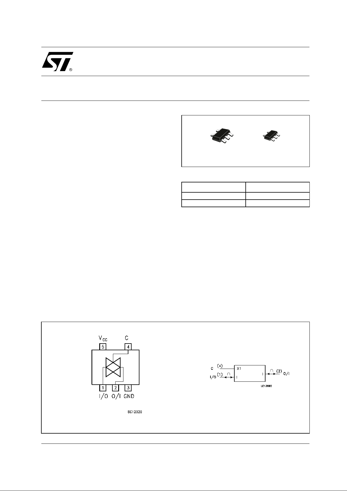
PIN CONNECTION AND IEC LOGIC SYMBOLS
ORDER CODES
PACKAGE T & R
SOT23-5L 74V1T66STR
SOT323-5L 74V1T66CTR
SOT323-5LSOT23-5L
74V1T66
2/11
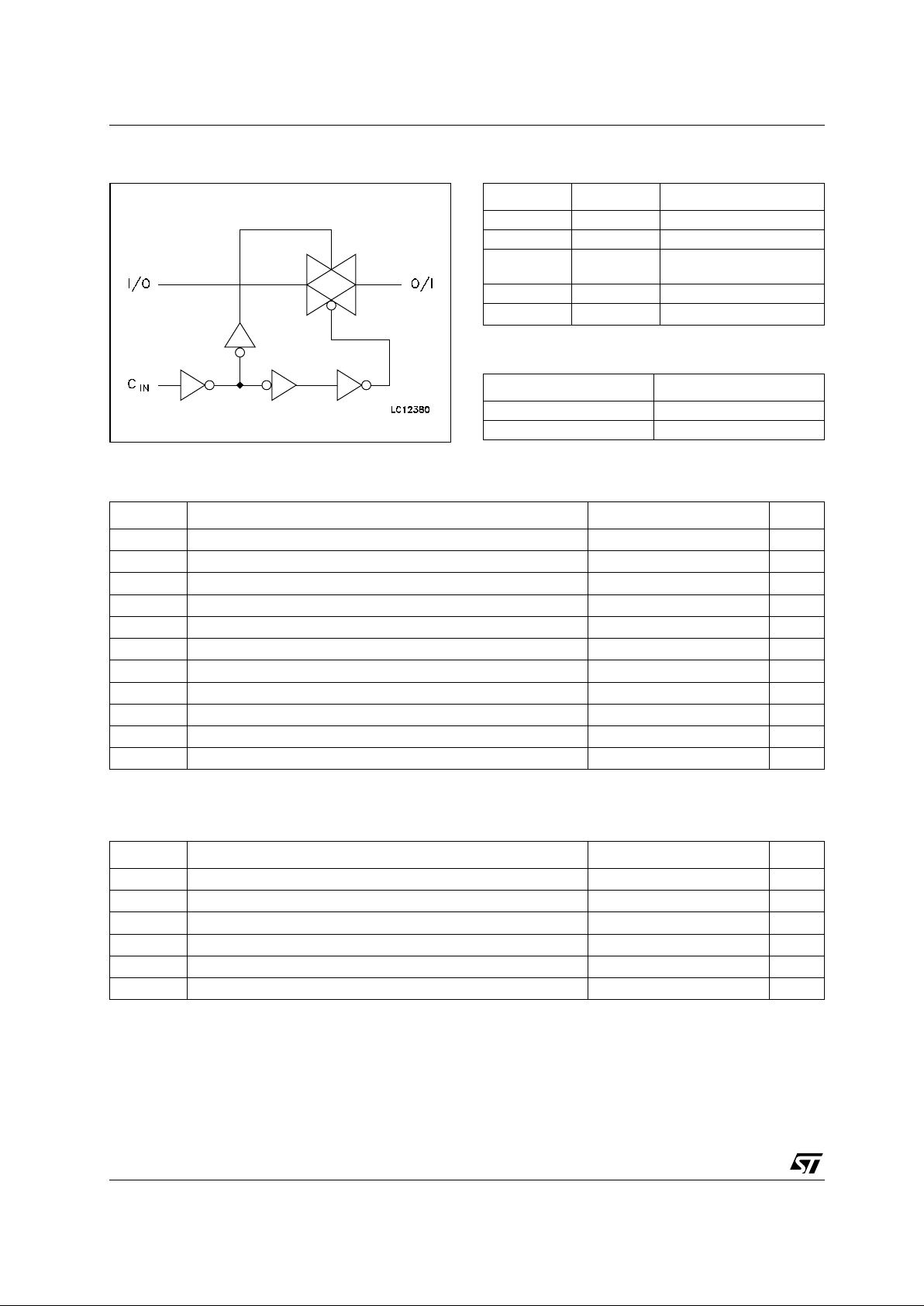
INPUT EQUIVALENT CIRCUIT PIN DESCRIPTION
TRUTH TABLE
* High Impedance Stat e
ABSOLUTE MAXIMUM RATI N GS
Absolute Maximum Ratings are those values beyond which damage to the device may occur. Functional operation under these conditions is
not implied
RECOMMENDED OPERATING CONDITIONS
1) VIN from 0.8V to 2V on control pin
PIN No SYMBOL NAME AND FUNCTION
1 I/O Independent Input/Output
2 O/I Independent Output/Input
4C
Enable Input (Active
HIGH)
3 GND Ground (0V)
5
V
CC
Positive Supply Voltage
CONTROL SWITCH FUNCTION
HON
L OFF *
Symbol Parameter Value Unit
V
CC
Supply Voltage
-0.5 to +7.0 V
V
I
DC Input Voltage -0.5 to VCC + 0.5
V
V
IC
DC Control Input Voltage
-0.5 to +7.0 V
V
O
DC Output Voltage -0.5 to VCC + 0.5
V
I
IK
DC Input Diode Current
± 20 mA
I
IK
DC Control Input Diode Current
- 20 mA
I
OK
DC Output Diode Current
± 20 mA
I
O
DC Output Current
± 50 mA
I
CC
or I
GND
DC VCC or Ground Current
± 50 mA
T
stg
Storage Temperature
-65 to +150 °C
T
L
Lead Temperature (10 sec)
300 °C
Symbol Parameter Value Unit
V
CC
Supply Voltage
4.5 to 5.5 V
V
I
Input Voltage 0 to V
CC
V
V
IC
Control Input Voltage
0 to 5.5 V
V
O
Output Voltage 0 to V
CC
V
T
op
Operating Temperature
-55 to 125 °C
dt/dv
Input Rise and Fall Time (note 1) V
CC
= 5.0V
0 to 20 ns/V
74V1T66
3/11
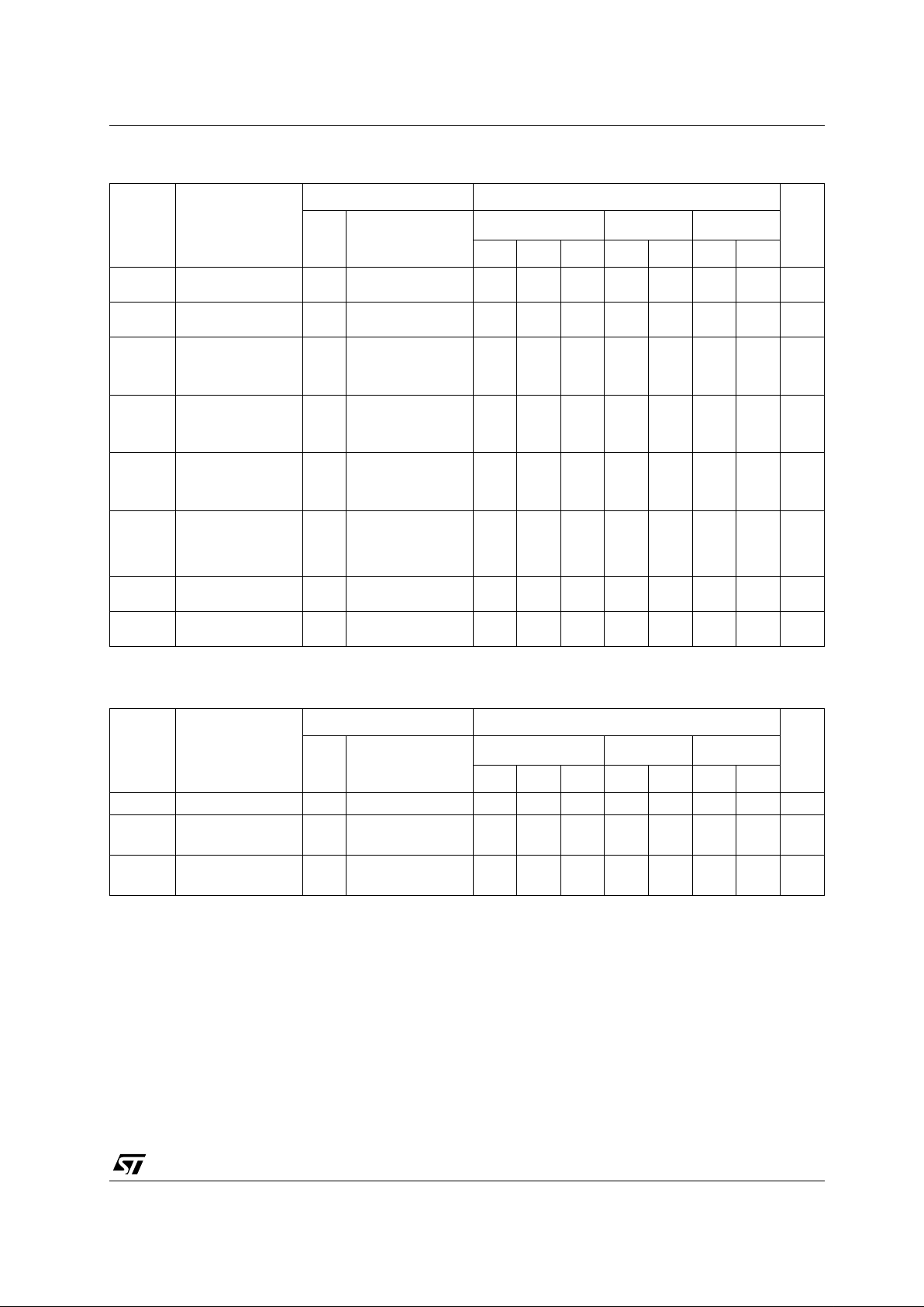
DC SPECIFICATIONS
(*) Vol tage range is 5V ± 0.5V
AC ELECTRICAL CHARACTERISTICS (CL = 50pF, Input tr = tf = 3ns)
(*) Vol tage range is 5. 0V ± 0.5V
Symbol Parameter
Test Condition Value
Unit
V
CC
(V)
T
A
= 25°C
-40 to 85°C -55 to 125°C
Min. Typ. Max. Min. Max. Min. Max.
V
IH
High Level Input
Voltage
5.0
(*)
222V
V
IL
Low Level Input
Voltage
5.0
(*)
0.8 0.8 0.8 V
R
ON
ON Resistance
5.0
(*)
VIC = VIH
V
I/O
= VCC to GND
I
I/O
≤ 1mA
7.5 10 12 14
V
R
ON
ON Resistance
5.0
(*)
VIC = VIH
V
I/O
= VCC or GND
I
I/O
≤ 1mA
6.5 8.5 10 12
V
I
OFF
Input/Output
Leakage Current
(SWITCH OFF)
5.5
VOS = VCC to GND
V
IS
= VCC to GND
V
IC
= V
IL
±0.1 ± 1 ± 5 µA
I
IZ
Switch Input
Leakage Current
(SWITCH ON,
OUTPUT OPEN)
5.5
V
OS
= VCC to GND
V
IC
= V
IH
±0.1 ± 1 ± 5 µA
I
IN
Control Input
Leakage Current
0 to
5.5
V
IC
= 5.5V or GND
± 0.1 ± 1.0 ± 1.0 µA
I
CC
Quiescent Supply
Current
5.5
V
I
= VCC or GND
11020µA
Symbol Parameter
Test Condition Value
Unit
V
CC
(V)
T
A
= 25°C
-40 to 85°C -55 to 125°C
Min. Typ. Max. Min. Max. Min. Max.
t
PD
Delay Time
5.0
(*)
tr = tf = 6ns
0.3 0.6 1.0 2.0 ns
t
PLZ
t
PHZ
Output Disable
Time
5.0
(*)
RL = 500 Ω
5.0 7.5 9.0 10.0 ns
t
PZL
t
PZH
Output Enable
Time
5.0
(*)
RL = 1 KΩ
2.0 4.0 5.0 7.0 ns
74V1T66
4/11
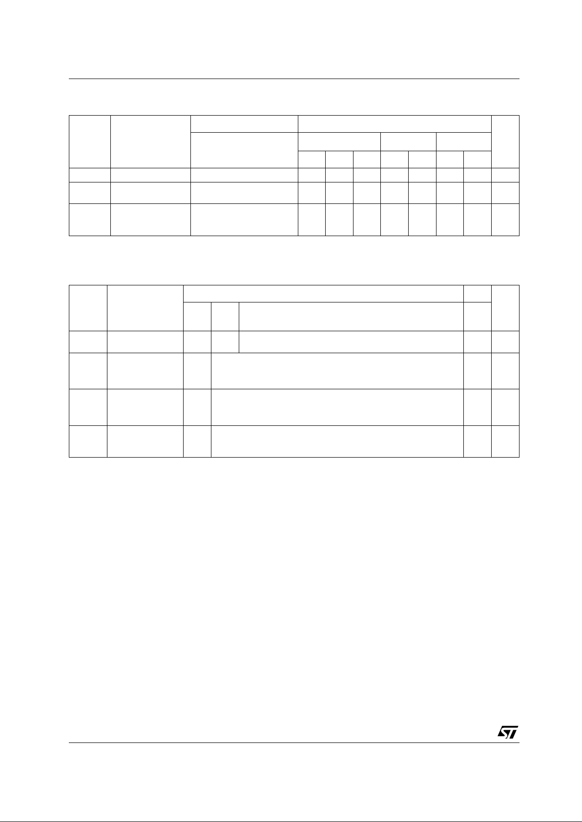
CAPACITIVE CHARACTERISTICS
1) CPD is defined as the value of the IC’s internal equivalent capacitance which is calculated from the operating current consumption without
load. (R ef er to Test Circ ui t). Averag e operatin g current can be obtained by t he following equation. I
CC(opr)
= CPD x VCC x fIN + I
CC
ANALOG SWITCH CHARACTERISTICS (GND = 0V; TA = 25°C)
(*) Vol tage range is 5. 0V ± 0.5V
Symbol Parameter
Test Condition Value
Unit
T
A
= 25°C
-40 to 85°C -55 to 125°C
Min. Typ. Max. Min. Max. Min. Max.
C
IN
Input Capacitance
3101010pF
C
I/O
Output
Capacitance
10 pF
C
PD
Power Dissipation
Capacitance
(note 1)
3pF
Symbol Parameter
Test Condition Value
Unit
V
CC
(V)
V
IN
(V
p-p
)
Typ.
Sine Wave
Distortion (THD)
5.0(*) 4
f
IN
= 1 KHz RL = 10 KΩ, CL = 50 pF
0.04 %
f
MAX
Frequency
Response
(Switch ON)
5.0(*) Adjust fIN voltage to obtain 0 dBm at VOS.
Increase f
IN
Frequency until dB meter reads -3dB
R
L
= 50Ω, CL = 10 pF
180 MHz
Feed through
Attenuation
(Switch OFF)
5.0(*) V
IN
is centered at VCC/2
Adjust f
IN
Voltage to obtained 0dBm at VIS
R
L
= 600Ω, CL = 50 pF, fIN = 1KHz sine wave
-60 dB
Crosstalk (Control
Input to Signal
Output)
5.0(*) R
L
= 600Ω, CL = 50 pF, fIN = 1KHz square wave
t
r
= tf = 6ns
60 mV
 Loading...