

SGS Thomson Microelectronics 74V1T66 Datasheet
■ HIGHSPEED:
=0.1ns(TYP.)at VCC=5V
t
PD
■ LOW POWERDISSIPATION:
I
=1 µA (MAX.)at TA=25oC
CC
■
LOW”ON”RESISTANCE:
=10Ω(TYP.)AT VCC=5VI
R
ON
■
SINE WAVEDISTOR TION
0.04%(TYP.)AT V
CC
=5Vf=1KHz
=100µA
I/O
DESCRIPTION
The 74V1T66 is an high-speed CMOS SINGLE
BILATERAL SWITCH fabricated in silicon gate
C2MOS technology. It achieves high speed
propagation delay and VERY LOW ON
resistances while maintaining true CMOS low
power consumption. This feature makes this part
ideal for battery-powered equipment. This
bilateral switch handles rail to rail analog and
digital signals that may vary across the full
power-supplyrange (from Vcc to Ground).
The C input is provided to control the switch and
it’s compatible with standard TTL output; the
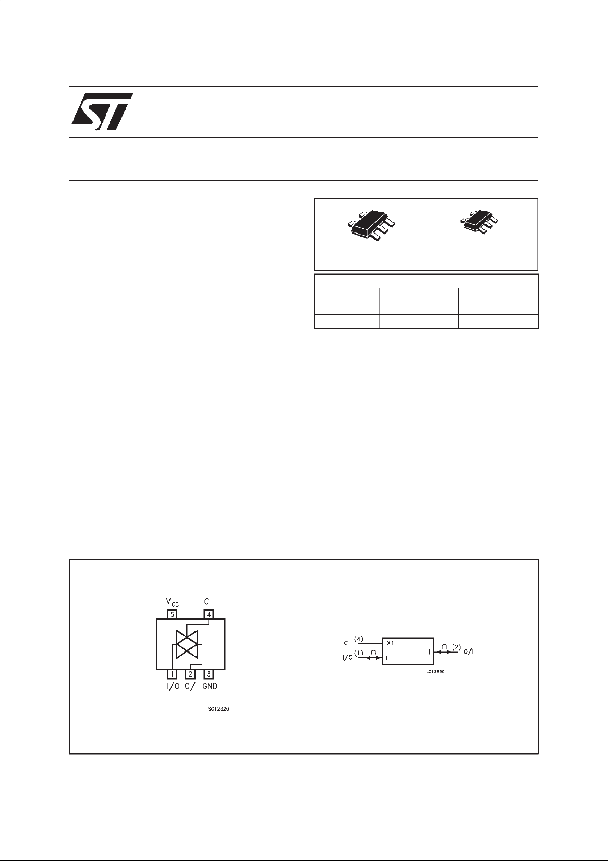
74V1T66
SINGLE BILATERAL SWITCH
SOT23-5L SC-70
ORDER CODES
PACKAGE TUBE T & R
SOT23-5L 74V1T66S-TR
SC-70 74V1T66C-TR
switchis ON whenthe C input is held high and off
when C is held low. It can be used in many
application as Battery Powered System, Audio
Signal Routing, Communications System, Test
Equipment. It’s available in the commercial
temperature range in SOT23-5L and SC-70-5L
package.
PIN CONNECTION AND IEC LOGIC SYMBOLS
February 2000
1/8
74V1T66
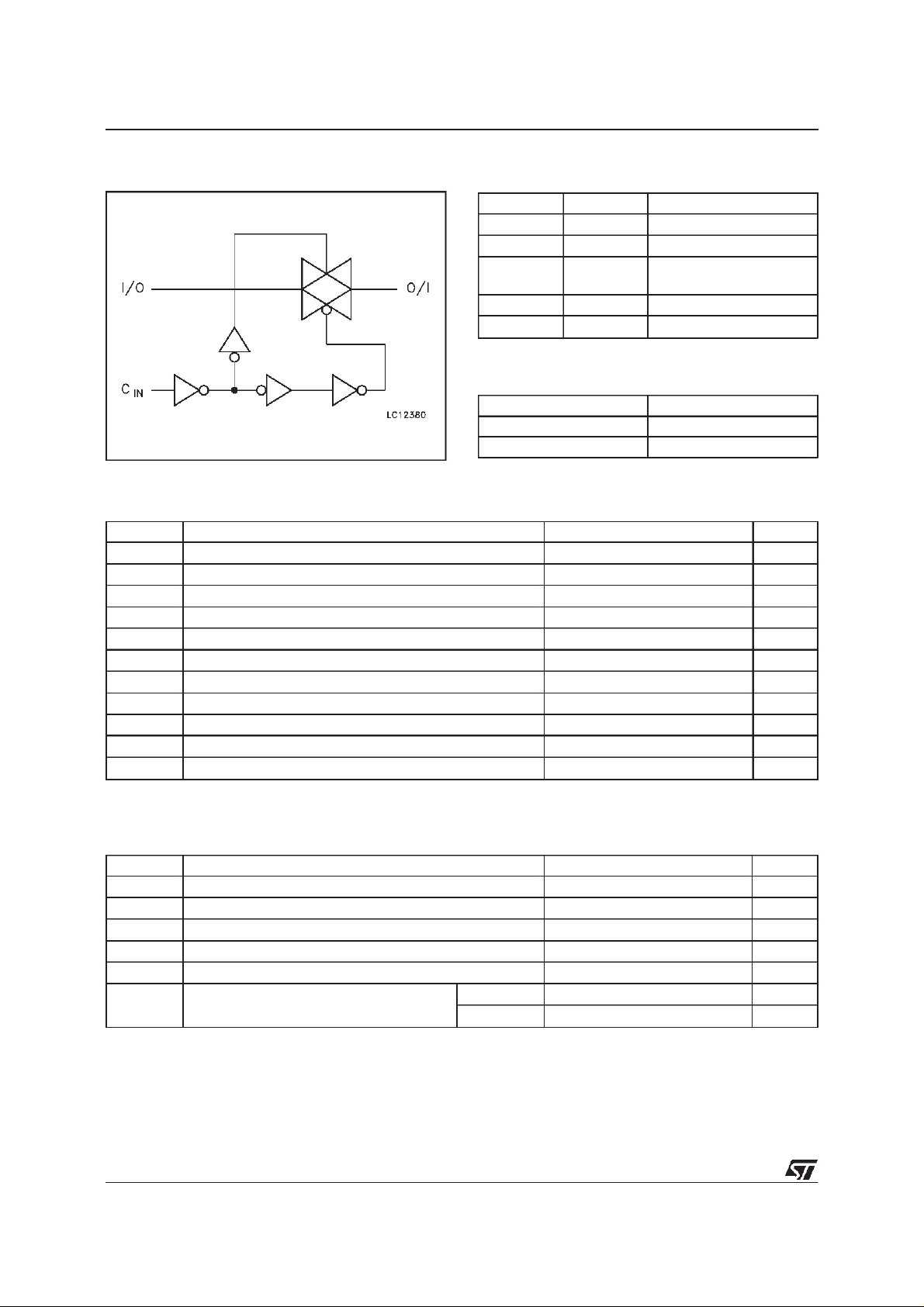
LOGICDIAGRAM
PIN DESCRIPTION
PI N No SYMB OL NAME AND F U NCTION
1 I/O Independent Input/Output
2 O/I Independent Output/Input
4 C Enable Input (Active
HIGH)
3 GND Ground (0V)
5V
CC
Positive Supply Voltage
TRUTH TABLE
CONT ROL SW I TCH F UNC T I ON
HON
L OFF
ABSOLUTE MAXIMUM RATINGS
Symb o l Para met er Val u e Uni t
V
V
V
V
I
I
I
OK
I
or I
I
CC
T
T
AbsoluteMaximumRatingsarethosevaluesbeyond whichdamagetothedevice mayoccur. Functionaloperationunderthesecondition isnotimplied.
Supply Voltage -0.5 to +7 V
CC
DC Input Voltage -0.5 to VCC+ 0.5 V
I
DC Control Input Voltage -0.5 to 7 V
IC
DC Output Voltage -0.5 to VCC+ 0.5 V
O
DC Input Diode Current ± 20 mA
IK
DC Control Input Diode Current - 20 mA
IK
DC Output Diode Current
DC Output Current ± 50 mA
O
DC VCCor Ground Current ± 50 mA
GND
Storage Temperature -65 to +150
stg
Lead Temperature (10 sec) 300
L
20 mA
±
o
C
o
C
RECOMMENDED OPERATINGCONDITIONS
Symb o l Para met er Value Un it
V
V
V
V
T
dt/dv Input Rise and Fall Time (note 1) V
1)VINfrom08V to2V
2/8
Supply Voltage 4.5 to 5.5 V
CC
Input Voltage 0 to V
I
Control Input Voltage 0 to 5.5 V
IC
Output Voltage 0 to V
O
Operating Temperature: -40 to +85
op
=5V 0 to 20 ns/V
CC
=3.3V 0 to 100 ns/V
V
CC
CC
CC
V
V
o
C
74V1T66
DC SPECIFICATIONS
Symb o l Parameter Test Co n ditions Val u e Uni t
=25oC -40 t o 85oC
T
A
Min. Typ. Max. Min. Max.
2.0 2.0 V
12 17 20 Ω
10 14 18
±0.1 ±1.0 µA
±0.1 ±1.0 µA
µ
High Level Input Voltage
V
IH
Low Level Input Voltage 0.8 0.8 V
V
IL
R
R
ON Resistance 5.0
ON
ON Resistance 5.0
ON
Input/Output Leakage
I
OFF
Current (SWITCH OFF)
Switch Input Leakage
I
IZ
Current (SWITCH ON,
OUTPUT OPEN)
Control Input Leakage
I
IN
Current
Quiescent Supply Current 5.5 VIC=VCCor GND 1 10
I
CC
(*) Voltagerange is 5V ±0.5V
V
CC
(V)
(*)
5.0
(*)
(*)
VIC=V
V
I/O=VCC
I
I/O
VIC=V
V
I/O=VCC
I
I/O
IH
to G ND
≤ 1m A
IH
or GND
≤ 1m A
5.5 VOS=VCCto GND
V
IS=VCC
V
IC=VIL
to G ND
5.5 VOS=VCCto GND
V
IC=VIH
0to
VIC= 5.5V or GND ±0.1 ±1.0 µA
5.5
Ω
A
AC ELECTRICAL CHARACTERISTICS
= 50 pF, Input tr=tf=3 ns)
(C
L
Symbol Parameter Test Co ndition Value Unit
V
CC
(V)
t
Delay Time 5.0
PD
Output Enable Time 5.0
t
PZL
t
PZH
t
Output Disable Time 5.0
PLZ
t
PHZ
C
Input Capacitance 5
IN
Switch Terminal
C
I/O
(*)
(*)
RL=1kΩ
(*)
RL=1k
Ω
Capacitance
Power Dissipation
C
PD
5.0 3 pF
Min. Typ. Max. Min. Max.
=25oC -40 t o 85oC
T
A
0.1 0.2 1.0 ns
2.0 4.0 5.0
5.0 7.5 9.0
10
ns
ns
pF
pF
Capacitance (note 1)
1)CPDisdefined as thevalueoftheIC’sinternalequivalentcapacitance whichiscalculatedfromtheoperating current consumption withoutload. (Referto
TestCircuit).Average operatingcurrent canbeobtained bythefollowingequation. I
(*) Voltagerange is 5V ±0.5V
(opr)= CPD• VCC•fIN+ICC(switch).
CC
3/8
 Loading...