

SGS Thomson Microelectronics 74V1T07STR, 74V1T07CTR Datasheet
1/9July 2001
■ HIGH SPEED: t
PD
= 4.3ns (TYP.) at VCC = 5V
■ LOW POWER DISSIPATION:
I
CC
= 1µA(MAX.) at TA=25°C
■ COMPA TIBLE WITH TTL OUTPUTS:
V
IH
= 2V (MIN), VIL = 0.8V (MAX)
■ POWER DOWN PROTECTION ON INPUT
■ OPERATING VOLTAGE RANGE:
V
CC
(OPR) = 4.5V to 5.5V
■ IMPROVED LATCH-UP IMMUNITY
DESCRIPTION
The 74V1T07 is an advanc ed high-speed CM OS
SINGLE BUFFER (OPEN DRAIN) fabricated with
sub-micron silicon gate and double-layer metal
wiring C
2
MOS technology.
The internal circuit is composed of 2 stages
including buffer output, which provide high no ise
immunity and stable output.
Power down protection is provided on inpu t an d 0
to 7V can be acce pted on inp ut with no rega rd to
the supply voltage. This device can be used to
interface 5V to 3V.
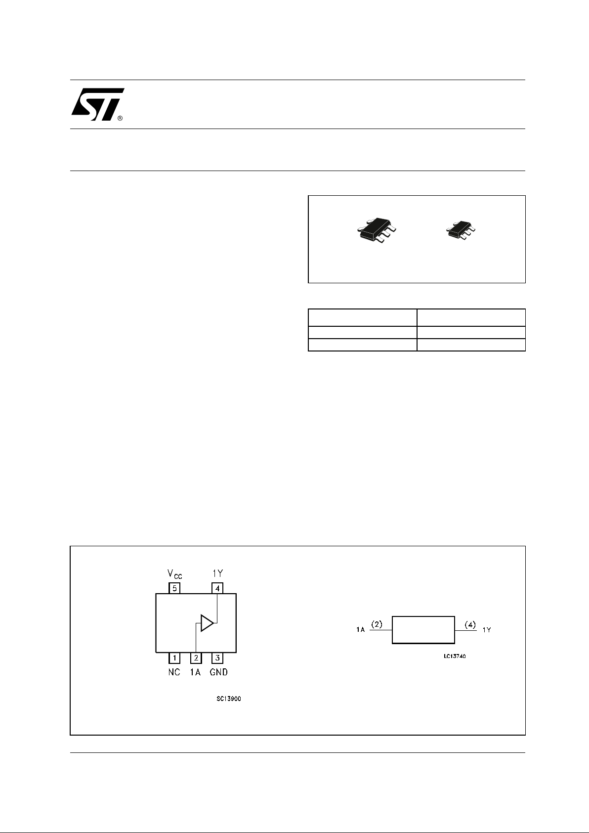
74V1T07
SINGLE BUFFER (OPEN DRAIN)
PIN CONNECTION AND IEC LOGIC SYMBOLS
ORDER CODES
PACKAGE T & R
SOT23-5L 74V1T07STR
SOT323-5L 74V1T07CTR
SOT323-5LSOT23-5L
74V1T07
2/9
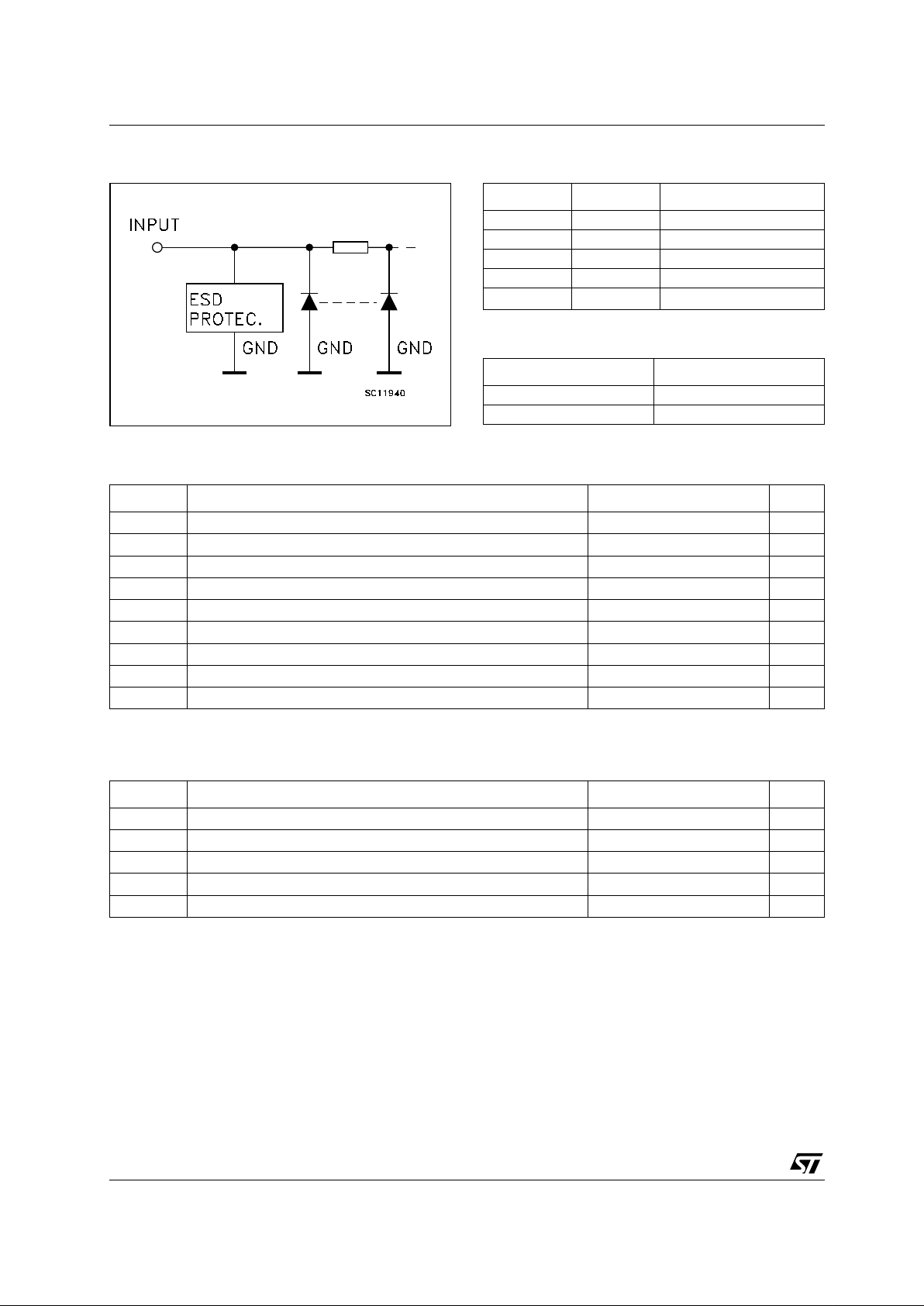
INPUT EQUIVALENT CIRCUIT PIN DESCRIPTION
TRUTH TABLE
Z: High Impedance
ABSOLUTE MAXIMUM RATINGS
Absolute Maximum Ratings are those values beyond which damage to the device may occur. Functional operation under these conditions is
not implied.
RECOMMENDED OPERATING CONDITIONS
1) VIN from 0.8V to 2V
PIN No SYMBOL NAME AND FUNCTION
1 NC Not Connected
2 1A Data Input
4 1Y Data Output
3 GND Ground (0V)
5
V
CC
Positive Supply Voltage
AY
LL
HZ
Symbol Parameter Value Unit
V
CC
Supply Voltage
-0.5 to +7.0 V
V
I
DC Input Voltage
-0.5 to +7.0 V
V
O
DC Output Voltage -0.5 to VCC + 0.5
V
I
IK
DC Input Diode Current
- 20 mA
I
OK
DC Output Diode Current
± 20 mA
I
O
DC Output Current
± 25 mA
I
CC
or I
GND
DC VCC or Ground Current
± 50 mA
T
stg
Storage Temperature
-65 to +150 °C
T
L
Lead Temperature (10 sec)
260 °C
Symbol Parameter Value Unit
V
CC
Supply Voltage
4.5 to 5.5 V
V
I
Input Voltage
0 to 5.5 V
V
O
Output Voltage 0 to V
CC
V
T
op
Operating Temperature
-55 to 125 °C
dt/dv
Input Rise and Fall Time (note 1) (V
CC
= 5.0 ± 0.5V)
0 to 20 ns/V
74V1T07
3/9
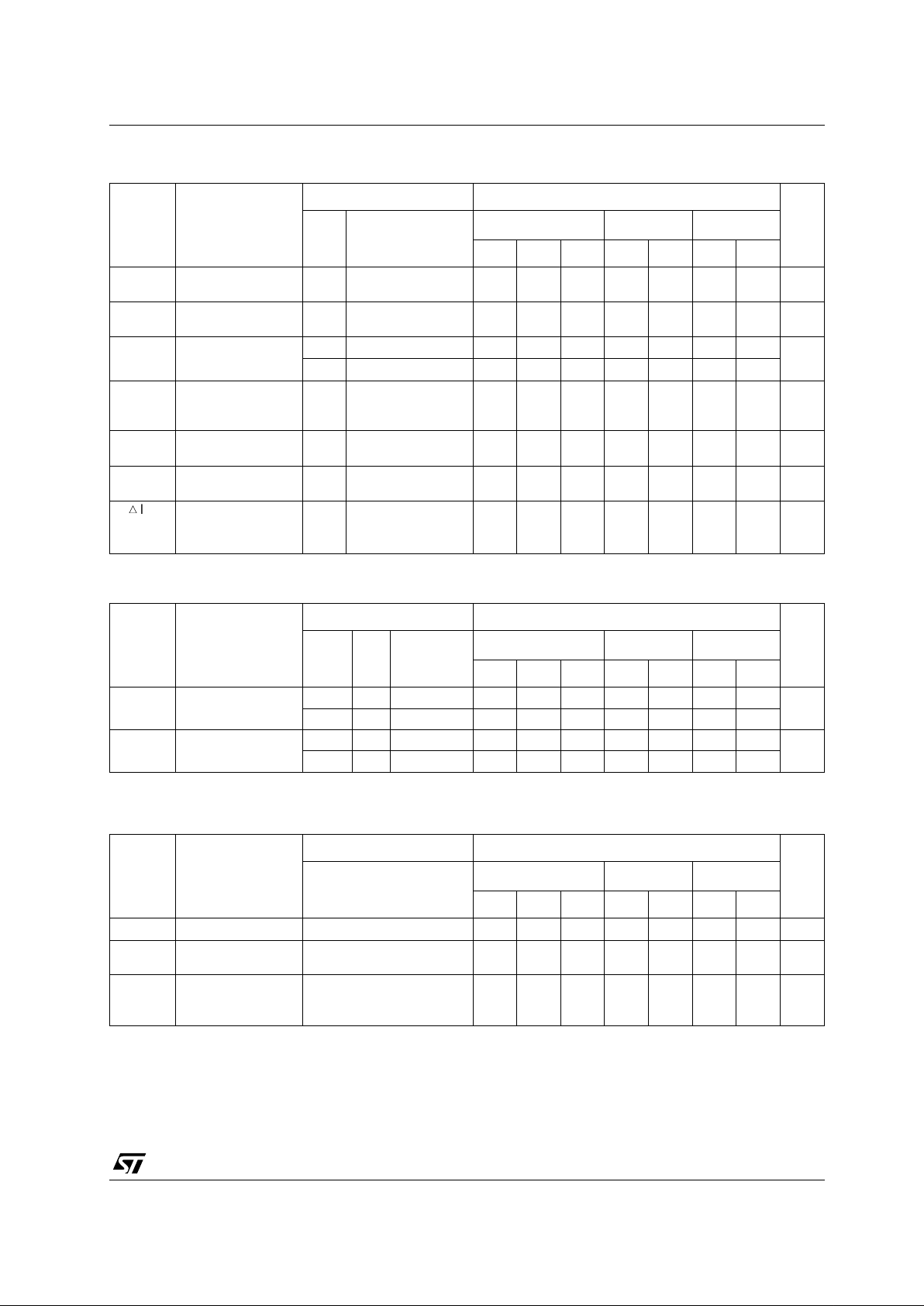
DC SPECIFICATIONS
AC ELECTRICAL CHARACTERISTICS (Input t
r
= tf = 3ns)
(*) Vol tage range is 5.0V ± 0.5V
CAPACITIVE CHARACTERISTICS
1) CPD is defined as the value of the IC’s internal equivalent capacitance which is calculated from the operating current consumption without
load. (R ef er to Test Circui t ). Average ope rating curre nt can be obtained by the follow i ng equation. I
CC(opr)
= CPD x VCC x fIN + I
CC
Symbol P arameter
Test Condition Value
Unit
V
CC
(V)
T
A
= 25°C
-40 to 85°C -55 to 125°C
Min. Typ. Max. Min. Max. Min. Max.
V
IH
High Level Input
Voltage
4.5 to
5.5
222V
V
IL
Low Level Input
Voltage
4.5 to
5.5
0.8 0.8 0.8 V
V
OL
Low Level Output
Voltage
4.5
IO=50 µA 0.0 0.1 0.1 0.1 V
4.5
I
O
=8 mA 0.36 0.44 0.55
I
OZ
High Impedance
Output Leakage
Current
5.5
VI = VIH or V
IL
VO = VCC or GND
±0.25 ± 2.5 ± 5.0 µA
I
I
Input Leakage
Current
0 to
5.5
V
I
= 5.5V or GND
± 0.1 ± 1.0 ± 1.0 µA
I
CC
Quiescent Supply
Current
5.5
V
I
= VCC or GND
11020µA
I
CC
Additional Worst
Case Supply
Current
5.5
One Input at 3.4V,
other input at V
CC
or GND
1.35 1.5 1.5 mA
Symbol Parameter
Test Condition Value
Unit
V
CC
(V)
C
L
(pF)
T
A
= 25°C
-40 to 85°C -55 to 125°C
Min. Typ. Max. Min. Max. Min. Max.
t
PZL
Enable Delay Time
5.0 (*) 15 3.7 7.0 1.0 8.0 1.0 9.0
ns
5.0 (*) 50 4.1 8.0 1.0 9.0 1.0 10.0
t
PLZ
Disable Delay Time
5.0 (*) 15 4.3 7.0 1.0 8.0 1.0 9.0
ns
5.0 (*) 50 4.7 8.0 1.0 9.0 1.0 10.0
Symbol Parameter
Test Condition Value
Unit
T
A
= 25°C
-40 to 85°C -55 to 125°C
Min. Typ. Max. Min. Max. Min. Max.
C
IN
Input Capacitance 4 10 10 10 pF
C
OUT
Output
Capacitance
5pF
C
PD
Power Dissipation
Capacitance
(note 1)
9pF
 Loading...