

1/9July 2001
■ HIGH SPEED: t
PD
=5.4ns (TYP.) at VCC = 5V
■ LOW POWER DISSIPATION:
I
CC
= 1µA(MAX.) at TA=25°C
■ COMPAT I B LE WITH TT L OUTPUTS:
V
IH
= 2V (MIN), VIL = 0.8V (MAX)
■ POWER DOWN PROTECTION ON INPUT
■ OPERATING VOLTAGE RANGE:
V
CC
(OPR) = 4.5V to 5.5V
■ IMPROVED LATCH-UP IMMUNITY
DESCRIPTION
The 74V1T05 is an advanc ed high-speed CM OS
SINGLE INVERTER (OPEN DRAIN) fabricated
with sub-micron silicon gate and double-layer
metal wiring C
2
MOS technology.
The internal circuit is composed of 3 stages
including buffer output, which provide high no ise
immunity and stable output.
Power down protection is provided on inpu t an d 0
to 7V can be acce pted on inp ut with no rega rd to
the supply voltage. This device can be used to
interface 5V to 3V.
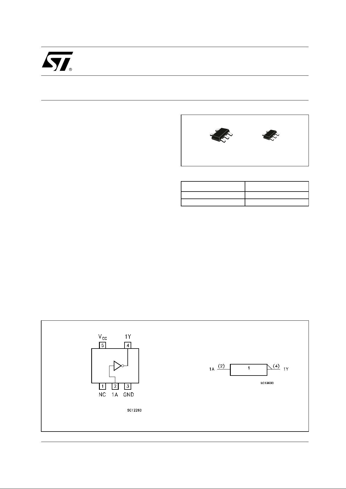
74V1T05
SINGLE INVERTER (OPEN DRAIN)
PIN CONNECTION AND IEC LOGIC SYMBOLS
ORDER CODES
PACKAGE T & R
SOT23-5L 74V1T05STR
SOT323-5L 74V1T05CTR
SOT323-5LSOT23-5L
74V1T05
2/9
INPUT EQUIVALENT CIRCUIT PIN DESCRIPTION
TRUTH TABLE
Z: High Impedance
ABSOLUTE MAXIMUM RATI N GS
Absolute Maximum Ratings are those values beyond which damage to the device may occur. Functional operation under these conditions is
not implied.
RECOMMENDED OPERATING CONDITIONS
1) VIN from 0.8V to 2V
PIN No SYMBOL NAME AND FUNCTION
1 NC Not Connected
2 1A Data Input
4 1Y Data Output
3 GND Ground (0V)
5
V
CC
Positive Supply Voltage
AY
LZ
HL
Symbol Parameter Value Unit
V
CC
Supply Voltage
-0.5 to +7.0 V
V
I
DC Input Voltage
-0.5 to +7.0 V
V
O
DC Output Voltage -0.5 to VCC + 0.5
V
I
IK
DC Input Diode Current
- 20 mA
I
OK
DC Output Diode Current
± 20 mA
I
O
DC Output Current
± 25 mA
I
CC
or I
GND
DC VCC or Ground Current
± 50 mA
T
stg
Storage Temperature
-65 to +150 °C
T
L
Lead Temperature (10 sec)
260 °C
Symbol Parameter Value Unit
V
CC
Supply Voltage
4.5 to 5.5 V
V
I
Input Voltage
0 to 5.5 V
V
O
Output Voltage 0 to V
CC
V
T
op
Operating Temperature
-55 to 125 °C
dt/dv
Input Rise and Fall Time (note 1) (V
CC
= 5.0 ± 0.5V)
0 to 20 ns/V
74V1T05
3/9
DC SPECIFICATIONS
AC ELECTRICAL CHARACTERISTICS (Input t
r
= tf = 3ns)
(*) Vol tage range is 5. 0V ± 0.5V
CAPACITIVE CHARACTERISTICS
1) CPD is defined as the value of the IC’s internal equivalent capacitance which is calculated from the operating current consumption without
load. (R ef er to Test Circuit). Average operating current can be obtained by t he following equation. I
CC(opr)
= CPD x VCC x fIN + I
CC
Symbol P arameter
Test Condition Value
Unit
V
CC
(V)
T
A
= 25°C
-40 to 85°C -55 to 125°C
Min. Typ. Max. Min. Max. Min. Max.
V
IH
High Level Input
Voltage
4.5 to
5.5
222V
V
IL
Low Level Input
Voltage
4.5 to
5.5
0.8 0.8 0.8 V
V
OL
Low Level Output
Voltage
4.5
IO=50 µA 0.0 0.1 0.1 0.1 V
4.5
I
O
=8 mA 0.36 0.44 0.55
I
OZ
High Impedance
Output Leakage
Current
5.5
VI = VIH or V
IL
VO = VCC or GND
±0.25 ± 2.5 ± 5.0 µA
I
I
Input Leakage
Current
0 to
5.5
V
I
= 5.5V or GND
± 0.1 ± 1.0 ± 1.0 µA
I
CC
Quiescent Supply
Current
5.5
V
I
= VCC or GND
11020µA
I
CC
Additional Worst
Case Supply
Current
5.5
One Input at 3.4V,
other input at V
CC
or GND
1.35 1.5 1.5 mA
Symbol Parameter
Test Condition Value
Unit
V
CC
(V)
C
L
(pF)
T
A
= 25°C
-40 to 85°C -55 to 125°C
Min. Typ. Max. Min. Max. Min. Max.
t
PZL
Enable Delay Time
5.0 (*) 15 3.7 7.0 1.0 8.0 1.0 9.0
ns
5.0 (*) 50 4.1 8.0 1.0 9.0 1.0 10.0
t
PLZ
Disable Delay Time
5.0 (*) 15 5.4 7.0 1.0 8.0 1.0 9.0
ns
5.0 (*) 50 5.8 8.0 1.0 9.0 1.0 10.0
Symbol Parameter
Test Condition Value
Unit
T
A
= 25°C
-40 to 85°C -55 to 125°C
Min. Typ. Max. Min. Max. Min. Max.
C
IN
Input Capacitance 4 10 10 10 pF
C
OUT
Output
Capacitance
5101010pF
C
PD
Power Dissipation
Capacitance
(note 1)
6pF

74V1T05
4/9
TEST CIRCUIT
CL = 15/50pF or e qui valent (i ncludes jig and probe capacitance)
R
1
= 1KΩ or equivalent
R
T
= Z
OUT
of pulse generator (typically 50Ω)
WAVEFORM: PROPAGATION DELAY (f=1MHz; 50% duty cycle)

74V1T05
5/9
DIM.
mm. mils
MIN. TYP MAX. MIN. TYP. M AX.
A 0.90 1.45 35.4 57.1
A1 0.00 0.15 0.0 5.9
A2 0.90 1.30 35.4 51.2
b 0.35 0.50 13.7 19.7
C 0.09 0.20 3.5 7.8
D 2.80 3.00 110.2 118.1
E 2.60 3.00 102.3 118.1
E1 1.50 1.75 59.0 68.8
e0.95 37.4
e1 1.9 74.8
L 0.35 0.55 13.7 21.6
SOT23-5L MECHANICAL DATA

74V1T05
6/9
DIM.
mm. mils
MIN. TYP MAX. MIN. TYP. M AX.
A 0.80 1.10 31.5 43.3
A1 0.00 0.10 0.0 3.9
A2 0.80 1.00 31.5 39.4
b 0.15 0.30 5.9 11.8
C 0.10 0.18 3.9 7.1
D 1.80 2.20 70.9 86.6
E 1.80 2.40 70.9 94.5
E1 1.15 1.35 45.3 53.1
e0.65 25.6
e1 1.3 51.2
L 0.10 0.30 3.9 11.8
SOT323-5L MECHANICAL DATA

74V1T05
7/9
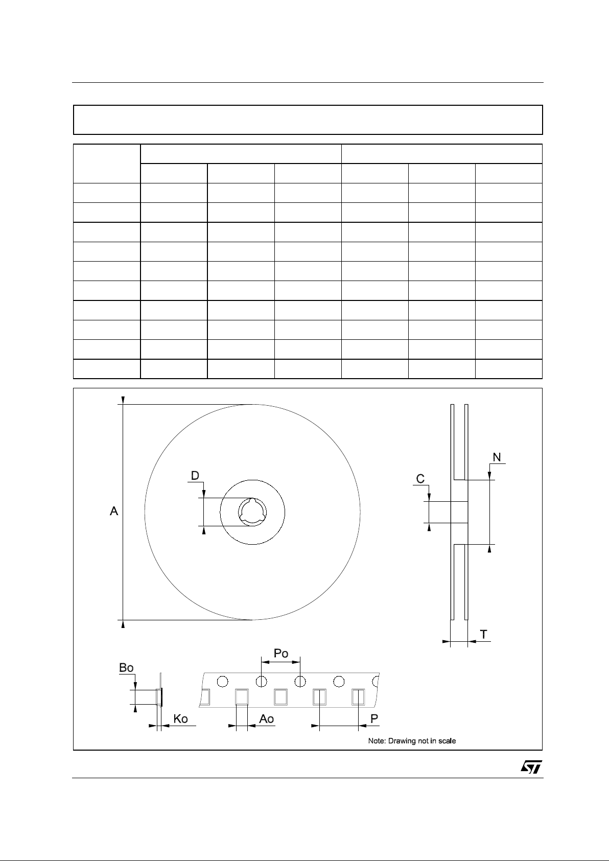
DIM.
mm. inch
MIN. TYP MAX. MIN. TYP. M AX.
A 180 7.086
C 12.8 13.0 13.2 0.504 0.512 0.519
D 20.2 0.795
N 60 2.362
T 14.4 0.567
Ao 3.13 3.23 3.33 0.123 0.127 0.131
Bo 3.07 3.17 3.27 0.120 0.124 0.128
Ko 1.27 1.37 1.47 0.050 0.054 0.0.58
Po 3.9 4.0 4.1 0.153 0.157 0.161
P 3.9 4.0 4.1 0.153 0.157 0.161
Tape & Reel SOT23-xL MECHANICAL DATA
74V1T05
8/9
DIM.
mm. inch
MIN. TYP MAX. MIN. TYP. M AX.
A 175 180 185 6.889 7.086 7.283
C 12.8 13 13.2 0.504 0.512 0.519
D 20.2 0.795
N 59.5 60 60.5 2.362
T 14.4 0.567
Ao 2.25 0.088
Bo 2.7 0.106
Ko 1.2 0.047
Po 3.98 4 4.2 0.156 0.157 0.165
P 3.98 4 4.2 0.156 0.157 0.165
Tape & Reel SOT323-xL MECHANICAL DATA

74V1T05
Information furnished is bel ieved to be accurate and reliable. However, STMicroe lectronics assumes no responsibility for the
consequences of use of such information nor for any infringement of patents or other rights of third parties which may result from
its use. No li cense is granted by i mp lica tion or otherwise under a n y patent or patent rig hts of STMicroelectronics. Spec ific at ions
mentioned in this publication ar e subject to change without notice. This publication supersedes and replaces all information
previously supplied. S TMicroelectronics products are not authorized for use as critica l components in life suppo rt devices or
systems without express written approval of STMicroelectronics.
© The ST logo is a registered trademark of STMicroelectronics
© 2001 STM icroelectronics - Printed in Italy - All Ri g h ts Reserv ed
STMicr o el ectronics G ROU P OF COMPANI E S
Australi a - Brazil - C hi na - Finlan d - F rance - Germ any - Hong Kon g - I ndi a - Italy - Japan - Malaysia - Malta - Morocco
Singapo re - Spain - Sweden - Swi t zerland - United Kingdom
© http://www.st.com
9/9
 Loading...