

1/9July 2001
■ HIGH SPEED: t
PD
= 3.5ns (TYP.) at VCC = 5V
■ LOW POWER DISSIPATION:
I
CC
= 1µA(MAX.) at TA=25°C
■ HIGH NOISE IMMUNITY:
V
NIH
= V
NIL
= 10% VCC (MIN.)
■ POWER DOWN PROTECTION ON INPUT
■ SYMMETRICAL OUTPUT IMPEDANCE:
|I
OH
| = IOL = 8mA (MIN) at VCC = 4.5V
■ BALANCED PROPAGATION DELAYS:
t
PLH
≅ t
PHL
■ OPERATING VOLTAGE RANGE:
V
CC
(OPR) = 2V to 5.5V
■ IMPROVED LATCH-UP IMMUNITY
DESCRIPTION
The 74V1GU04 is an advanced high-speed
CMOS SINGLE INVERTER (SINGLE STAGE)
fabricated with sub-micron silicon gate and
double-layer metal wiring C
2
MOS technology.
The internal circuit is composed of a single stages
inverter, then an unbuffered output.
it can be used in analog application such a crystal
oscillator.
Power down protection is provided on inpu t an d 0
to 7V can be acce pted on inp ut with no rega rd to
the supply voltage. This device can be used to
interface 5V to 3V.
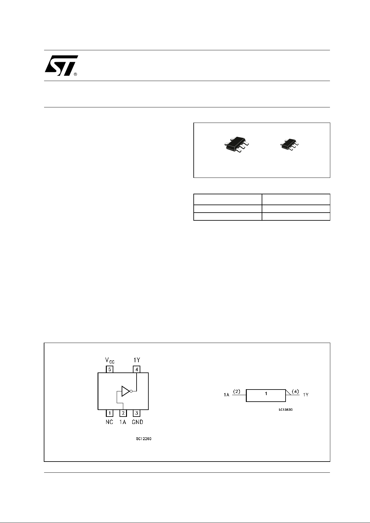
74V1GU04
SINGLE INVERTER (SINGLE STAGE)
PIN CONNECTION AND IEC LOGIC SYMBOLS
ORDER CODES
PACKAGE T & R
SOT23-5L 74V1GU04STR
SOT323-5L 74V1GU04CTR
SOT323-5LSOT23-5L
74V1GU04
2/9
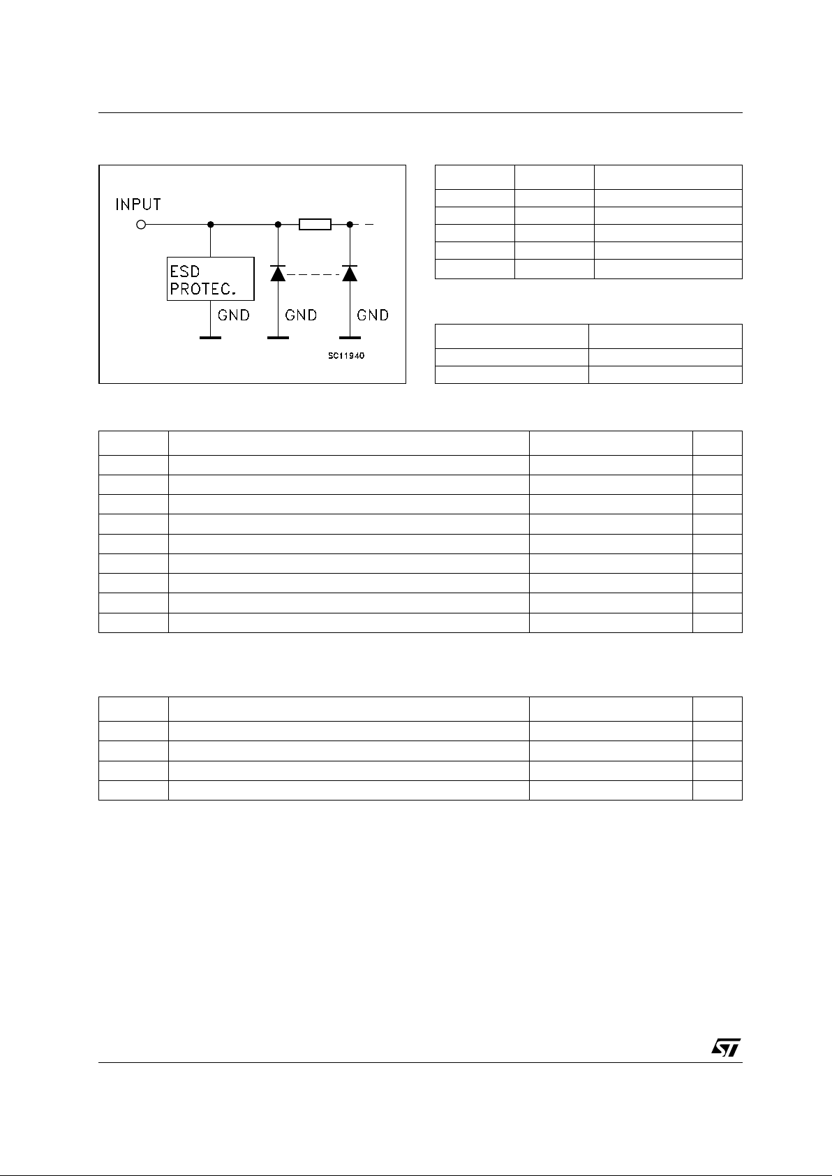
INPUT EQUIVALENT CIRCUIT PIN DESCRIPTION
TRUTH TABLE
ABSOLUTE MAXIMUM RATINGS
Absolute Maximum Ratings are those values beyond which damage to the device may occur. Functional operation under these conditions is
not implied.
RECOMMENDED OPERATING CONDITIONS
PIN No SYMBOL NAME AND FUNCTION
1 NC Not Connected
2 1A Data Input
4 1Y Data Output
3 GND Ground (0V)
5
V
CC
Positive Supply Voltage
AY
LH
HL
Symbol Parameter Value Unit
V
CC
Supply Voltage
-0.5 to +7.0 V
V
I
DC Input Voltage
-0.5 to +7.0 V
V
O
DC Output Voltage -0.5 to VCC + 0.5
V
I
IK
DC Input Diode Current
- 20 mA
I
OK
DC Output Diode Current
± 20 mA
I
O
DC Output Current
± 25 mA
I
CC
or I
GND
DC VCC or Ground Current
± 50 mA
T
stg
Storage Temperature
-65 to +150 °C
T
L
Lead Temperature (10 sec)
260 °C
Symbol Parameter Value Unit
V
CC
Supply Voltage
2 to 5.5 V
V
I
Input Voltage
0 to 5.5 V
V
O
Output Voltage 0 to V
CC
V
T
op
Operating Temperature
-55 to 125 °C
74V1GU04
3/9
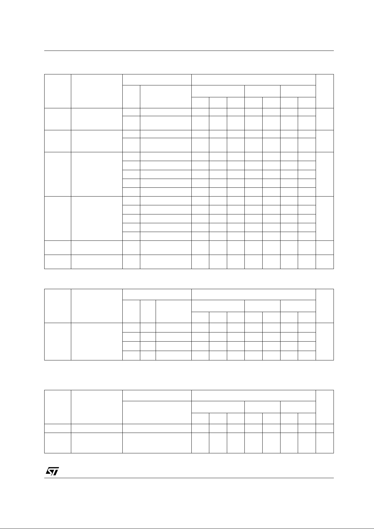
DC SPECIFICATIONS
AC ELECTRICAL CHARACTERISTICS (Input t
r
= tf = 3ns)
(*) Vol tage range is 3.3V ± 0.3V
(**) Voltage range is 5.0V ±
0.5V
CAPACITIVE CHARACTERISTICS
1) CPD is defined as the value of the IC’s internal equivalent capacitance which is calculated from the operating current consumption without
load. (R ef er to Test Circui t ). Average ope rating curre nt can be obtained by the follow i ng equation. I
CC(opr)
= CPD x VCC x fIN + I
CC
Symbol P arameter
Test Condition Value
Unit
V
CC
(V)
T
A
= 25°C
-40 to 85°C -55 to 125°C
Min. Typ. Max. Min. Max. Min. Max.
V
IH
High Level Input
Voltage
2.0 1.7 1.7 1.7
V
3.0 to
5.5
0.8V
CC
0.8V
CC
0.8V
CC
V
IL
Low Level Input
Voltage
2.0 0.3 0.3 0.3
V
3.0 to
5.5
0.2V
CC
0.2V
CC
0.2V
CC
V
OH
High Level Output
Voltage
2.0
I
O
=-50 µA
1.8 2.0 1.8 1.8
V
3.0
I
O
=-50 µA
2.7 3.0 2.7 2.7
4.5
I
O
=-50 µA
4.0 4.5 4.0 4.0
3.0
I
O
=-4 mA
2.58 2.48 2.4
4.5
I
O
=-8 mA
3.94 3.8 3.7
V
OL
Low Level Output
Voltage
2.0
IO=50 µA
0.0 0.2 0.2 0.2
V
3.0
I
O
=50 µA
0.0 0.3 0.3 0.3
4.5
I
O
=50 µA
0.0 0.5 0.5 0.5
3.0
I
O
=4 mA
0.36 0.44 0.55
4.5
I
O
=8 mA
0.36 0.44 0.55
I
I
Input Leakage
Current
0 to
5.5
V
I
= 5.5V or GND
± 0.1 ± 1 ± 1 µA
I
CC
Quiescent Supply
Current
5.5
V
I
= VCC or GND
11020µA
Symbol Parameter
Test Condition Value
Unit
V
CC
(V)
C
L
(pF)
T
A
= 25°C
-40 to 85°C -55 to 125°C
Min. Typ. Max. Min. Max. Min. Max.
t
PLH tPHL
Propagation Delay
Time
3.3
(*)
15 4.4 6.5 1.0 8.0 1.0 9.0
ns
3.3
(*)
50 4.8 7.0 1.0 9.0 1.0 10.0
5.0
(**)
15 3.5 5.5 1.0 6.0 1.0 7.5
5.0
(**)
50 4.1 6.0 1.0 7.0 1.0 8.0
Symbol Parameter
Test Condition Value
Unit
T
A
= 25°C
-40 to 85°C -55 to 125°C
Min. Typ. Max. Min. Max. Min. Max.
C
IN
Input Capacitance
5101010pF
C
PD
Power Dissipation
Capacitance
(note 1)
10 pF
 Loading...