

74V1G7 7
SINGLE D-TYPE LATCH
■ HIGH SPEED: t
■ LOW POWER DISSIPATION:
I
= 1µA(MAX.) at TA=25°C
CC
■ HIGH NOISE IMMUNITY:
V
= V
NIH
■ POWER DOWN PROTECTION ON INPUTS
■ SYMMETRICAL OUTPUT IMPEDANCE:
|I
| = IOL = 8mA (MIN) at VCC = 4.5V
OH
■ BALANCED PROPAGATION DELAYS:
t
≅ t
PLH
■ OPERATING VOLTAGE RANGE:
V
(OPR) = 2V to 5.5V
CC
■ IMPROVED LATCH-UP IMMUNITY
= 28% VCC (MIN.)
NIL
PHL
= 4.4ns (TYP.) at VCC = 5V
PD
DESCRIPTION
The 74V1G77 is an advanced high-speed CMOS
SINGLE D-TYPE LATCH fabricated with
sub-micron silicon gate and double-layer metal
wiring C
2
MOS technology. It is designed to
operate from 2V to 5.5V, making this device ideal
for portable applications.
The single D-Type latch is controlled by a Latch
Enable Input (LE ).
While the LE in put is held at a high level, the Q
output will follow the data input precisely. When
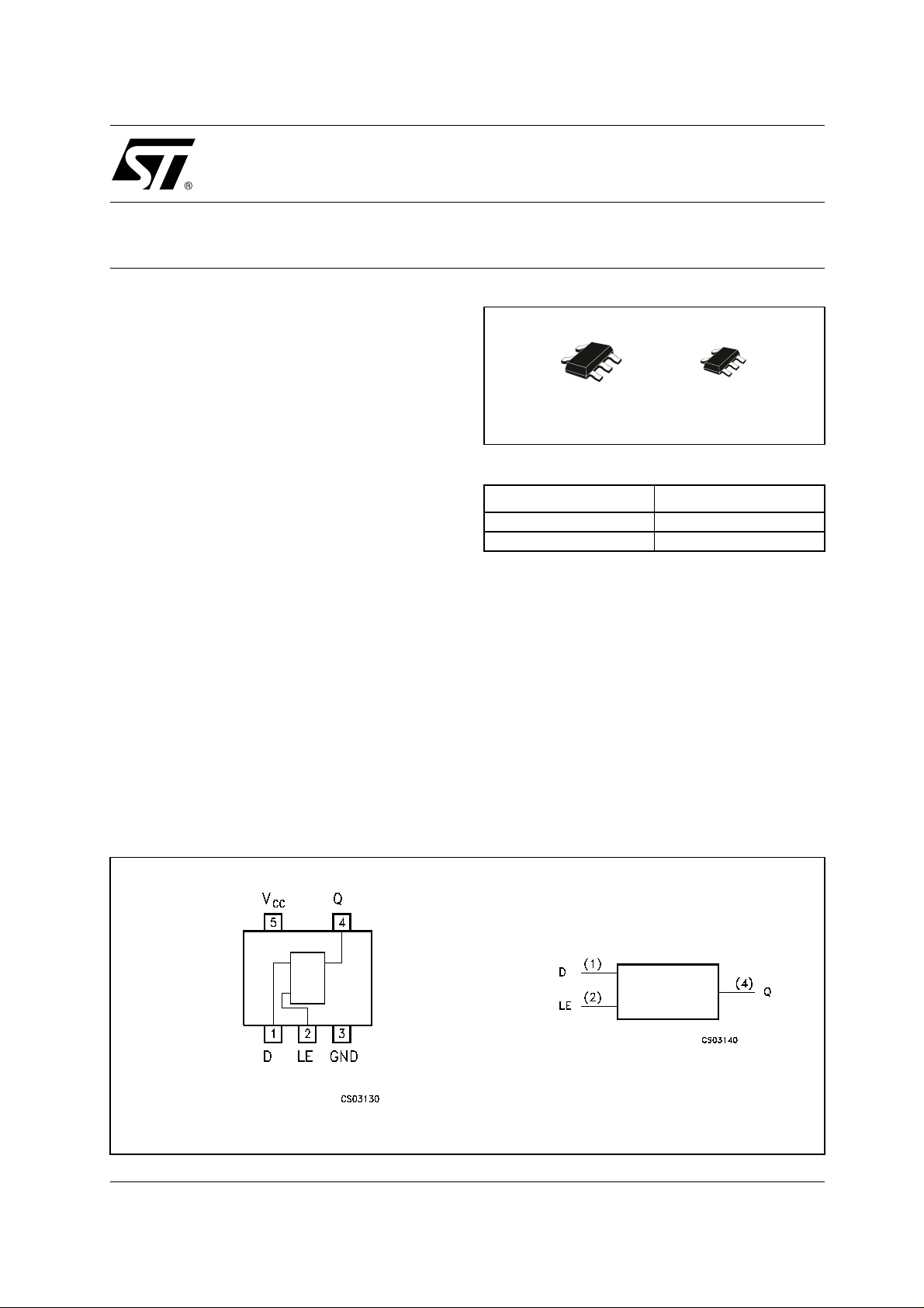
SOT323-5LSOT23-5L
ORDER CODES
PACKAGE T & R
SOT23-5L 74V1G77STR
SOT323-5L 74V1G77CTR
the LE input is taken lo w the Q output is latched
precisely at the logic level of D input data.
Power down protection is provided on in puts and
0 to 7V c an be accepted on inputs with no regard
to the supply voltage. This device can be used to
interface 5V to 3V. It’s available in the commercial
and extended temperature range.
All inputs and output are equippe d with prot ection
circuits against stati c disc harge , giving t hem ES D
immunity and transient excess voltage.
PIN CONNECTION AND IEC LOGIC SYMBOLS
1/10July 2001
74V1G77
INPUT EQUIVALENT CIRCUIT PIN DESCRIPTION
PIN No SYMBOL NAME QND FUNCTION
1 D Data Input
2 LE Latch Enable Input
4 Q Data Output
3 GND Ground (0V)
5
V
CC
TRUTH TABLE
DLEQ
L L No Change *
H L No Change *
LHQn
HHQn
(*) Q output is latched at the time when the le input is taken low logic
level.
ABSOLUTE MAXIMUM RATINGS
Symbol Parameter Value Unit
V
V
V
I
I
OK
I
I
or I
CC
T
T
Absolute Maximum Ratings are those values beyond which damage to the device may occur. Functional operation under these conditions is
not implied.
Supply Voltage
CC
DC Input Voltage
I
DC Output Voltage -0.5 to VCC + 0.5
O
DC Input Diode Current
IK
DC Output Diode Current
DC Output Current
O
DC VCC or Ground Current
GND
Storage Temperature
stg
Lead Temperature (10 sec)
L
Positive Supply Voltage
-0.5 to +7.0 V
-0.5 to +7.0 V
V
- 20 mA
± 20 mA
± 25 mA
± 50 mA
-65 to +150 °C
260 °C
RECOMMENDED OPERATING CONDITIONS
Symbol Parameter Value Unit
V
V
V
T
dt/dv
1) VIN from 30 % to 70% of V
2/10
Supply Voltage
CC
Input Voltage
I
Output Voltage 0 to V
O
Operating Temperature
op
Input Rise and Fall Time (note 1) (V
(V
CC
= 3.3 ± 0.3V)
CC
= 5.0 ± 0.5V)
CC
2 to 5.5 V
0 to 5.5 V
CC
-55 to 125 °C
0 to 100
0 to 20
V
ns/V
ns/V
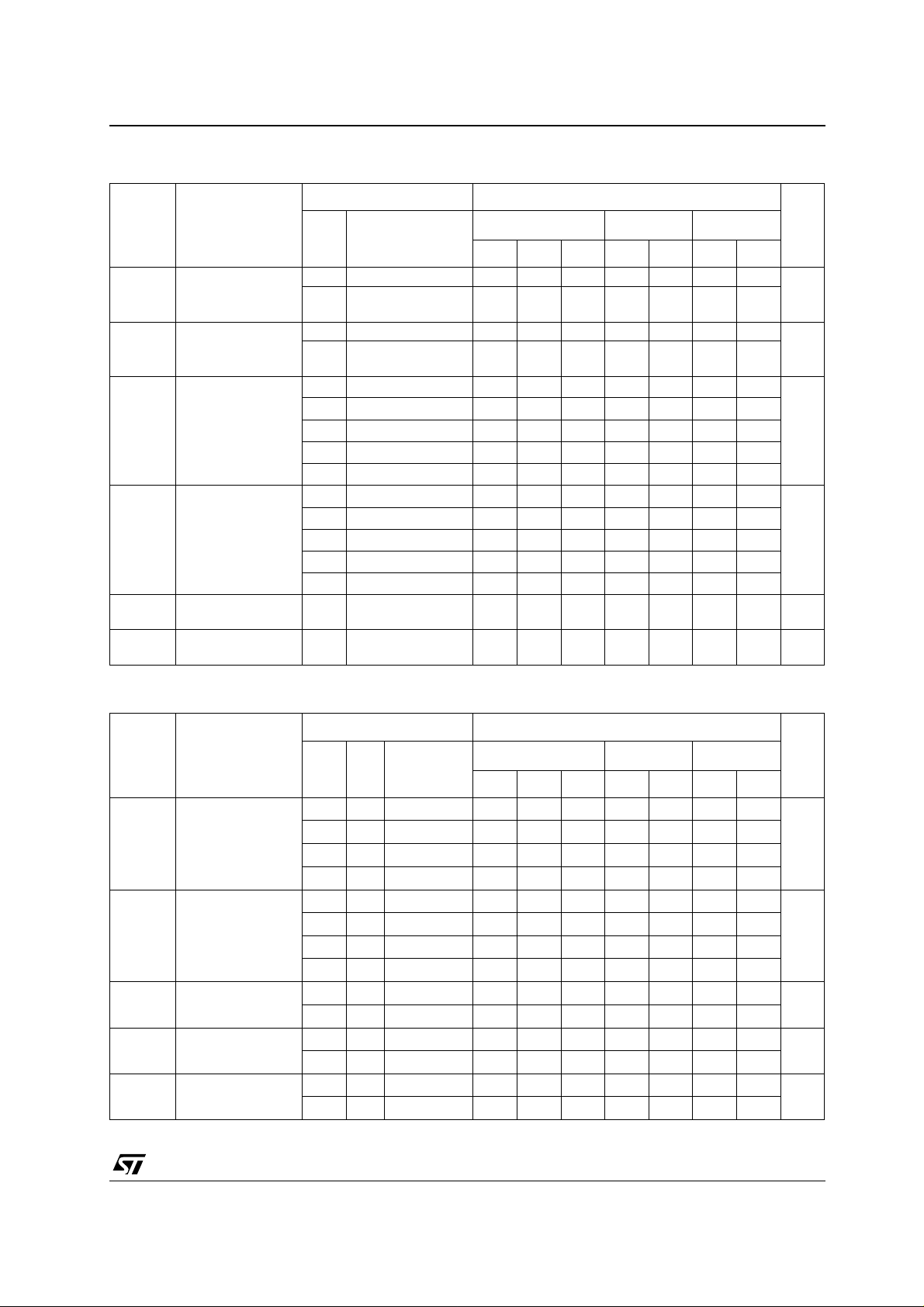
DC SPECIFICATIONS
Symbol Parameter
V
V
V
V
I
High Level Input
IH
Voltage
Low Level Input
IL
Voltage
High Level Output
OH
Voltage
Low Level Output
OL
Voltage
I
Input Leakage
I
Current
Quiescent Supply
CC
Current
Test Condition Value
V
(V)
CC
= 25°C
A
Min. Typ. Max. Min. Max. Min. Max.
-40 to 85°C -55 to 125°C
T
2.0 1.5 1.5 1.5
3.0 to
5.5
0.7V
CC
0.7V
CC
0.7V
CC
2.0 0.5 0.5 0.5
3.0 to
5.5
2.0
3.0
4.5
3.0
4.5
2.0
3.0
4.5
3.0
4.5
0 to
5.5
5.5
=-50 µA
I
O
I
=-50 µA
O
I
=-50 µA
O
I
=-4 mA
O
I
=-8 mA
O
IO=50 µA
I
=50 µA
O
I
=50 µA
O
I
=4 mA
O
I
=8 mA
O
V
= 5.5V or GND
I
= VCC or GND
V
I
1.9 2.0 1.9 1.9
2.9 3.0 2.9 2.9
4.4 4.5 4.4 4.4
2.58 2.48 2.4
3.94 3.8 3.7
0.3V
CC
0.3V
CC
0.0 0.1 0.1 0.1
0.0 0.1 0.1 0.1
0.0 0.1 0.1 0.1
0.36 0.44 0.55
0.36 0.44 0.55
± 0.1 ± 1 ± 1 µA
11020µA
74V1G77
Unit
0.3V
CC
V
V
V
V
AC ELECTRICAL CHARACTERISTICS (Input t
Test Condition Value
Symbol Parameter
t
PLH tPHL
t
PLH tPHL
(*) Vol tage range is 3.3V ± 0.3V
(**) Voltage range is 5.0V ±
Propagation Delay
Time LE to Q
Propagation Delay
Time D to Q
LE Pulse Width,
t
W
HIGH
Setup Time D to
t
s
LE, HIGH or LOW
Hold Time D to LE,
t
h
HIGH or LOW
0.5V
3.3
3.3
5.0
5.0
3.3
3.3
5.0
5.0
3.3
5.0
3.3
5.0
3.3
5.0
C
V
CC
(V)
L
(pF)
(*)
15 6.2 9.0 1.0 10.5 1.0 11.5
(*)
50 6.8 10.0 1.0 11.5 1.0 13.0
(**)
15 4.4 6.5 1.0 7.5 1.0 8.5
(**)
50 4.8 7.0 1.0 8.0 1.0 9.0
(*)
15 7.2 10.0 1.0 11.5 1.0 13.0
(*)
50 7.9 11.0 1.0 12.5 1.0 14.0
(**)
15 4.4 6.5 1.0 7.5 1.0 8.5
(**)
50 4.8 7.0 1.0 8.0 1.0 9.0
(*)
(**)
(*)
(**)
(*)
(**)
= tf = 3ns)
r
T
= 25°C
A
-40 to 85°C -55 to 125°C
Min. Typ. Max. Min. Max. Min. Max.
4.0 4.0 4.0
3.0 3.0 3.0
3.0 3.0 3.0
2.0 2.0 2.0
1.0 1.0 1.0
1.0 1.0 1.0
Unit
ns
ns
ns
ns
ns
3/10
 Loading...