

1/9July 2001
■ HIGH SPEED: t
PD
= 4.3ns (TYP.) at VCC = 5V
■ LOW POWER DISSIPATION:
I
CC
= 1µA(MAX.) at TA=25°C
■ TYPI C AL HYSTERES I S: V
h
=1V at VCC=4.5V
■ POWER DOWN PROTECTION ON INPUT
■ SYMMETRICAL OUTPUT IMPEDANCE:
|I
OH
| = IOL = 8mA (MIN) at VCC=4.5V
■ BALANCED PROPAGATION DELAYS:
t
PLH
≅ t
PHL
■
OPERATING VOLTAGE RANGE:
V
CC
(OPR) = 2V to 5.5V
■ IMPROVED LATCH-UP IMMUNITY
DESCRIPTION
The 74V1G14 is an advanced high-speed CMOS
SINGLE SCHMITT INVERTER fabricated with
sub-micron silicon gate and double-layer metal
wiring C
2
MOS technology.
The internal circuit is composed of 3 stages
including buffer output, which provide high no ise
immunity and stable output.
Power down protection is provided on inpu t an d 0
to 7V can be acce pted on inp ut with no rega rd to
the supply voltage. This device can be used to
interface 5V to 3V . Pin conf iguration and function
are the same as those of the 74V1G04 but the
74V1G14 has hysteresis.
This together with its schmitt trigger function
allows it to be used on line receivers with slow
rise/fall input signals.
The input is equipped with protection circuits
against static discharge, giving it ESD immunity
and transient excess voltage.
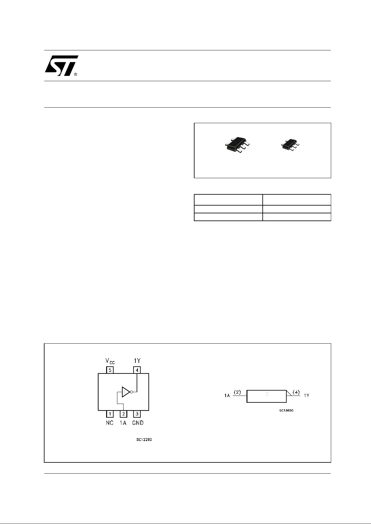
74V1G1 4
SINGLE SCH MITT INVERTER
PIN CONNECTION AND IEC LOGIC SYMBOLS
ORDER CODES
PACKAGE T & R
SOT23-5L 74V1G14STR
SOT323-5L 74V1G14CTR
SOT323-5LSOT23-5L
74V1G14
2/9
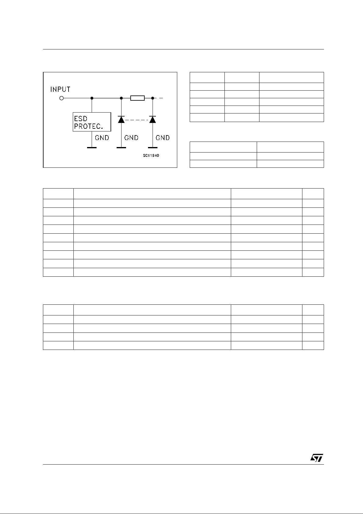
INPUT EQUIVALENT CIRCUIT PIN DESCRIPTION
TRUTH TABLE
ABSOLUTE MAXIMUM RATINGS
Absolute Maximum Ratings are those values beyond which damage to the device may occur. Functional operation under these conditions is
not implied.
RECOMMENDED OPERATING CONDITIONS
PIN No SYMBOL NAME AND FUNCTION
1 NC Not Connected
2 1A Data Input
4 1Y Data Output
3 GND Ground (0V)
5
V
CC
Positive Supply Voltage
AY
LH
HL
Symbol Parameter Value Unit
V
CC
Supply Voltage
-0.5 to +7.0 V
V
I
DC Input Voltage
-0.5 to +7.0 V
V
O
DC Output Voltage -0.5 to VCC + 0.5
V
I
IK
DC Input Diode Current
- 20 mA
I
OK
DC Output Diode Current
± 20 mA
I
O
DC Output Current
± 25 mA
I
CC
or I
GND
DC VCC or Ground Current
± 50 mA
T
stg
Storage Temperature
-65 to +150 °C
T
L
Lead Temperature (10 sec)
260 °C
Symbol Parameter Value Unit
V
CC
Supply Voltage
2 to 5.5 V
V
I
Input Voltage
0 to 5.5 V
V
O
Output Voltage 0 to V
CC
V
T
op
Operating Temperature
-55 to 125 °C
74V1G14
3/9
DC SPECIFICATIONS
AC ELECTRICAL CHARACTERISTICS (Input t
r
= tf = 3ns)
(*) Vol tage range is 3.3V ± 0.3V
(**) Voltage range is 5.0V ±
0.5V
Symbol Parameter
Test Condition Value
Unit
V
CC
(V)
T
A
= 25°C
-40 to 85°C -55 to 125°C
Min. Typ. Max. Min. Max. Min. Max.
V
t+
High Level
Threshold Voltage
3.0 1.2 2.2 1.2 2.2 1.2 2.2
V4.5 1.75 3.15 1.75 3.15 1.75 3.15
5.5 2.15 3.85 2.15 3.85 2.15 3.85
V
t-
Low Level
Threshold Voltage
3.0 0.9 1.9 0.9 1.9 0.9 1.9
V4.5 1.35 2.75 1.35 2.75 1.35 2.75
5.5 1.65 3.35 1.65 3.35 1.65 3.35
V
h
Hysteresis Voltage 3.0 0.3 1.2 0.3 1.2 0.3 1.2
V4.5 0.4 1.4 0.4 1.4 0.4 1.4
5.5 0.5 1.6 0.5 1.6 0.5 1.6
V
OH
High Level Output
Voltage
2.0
I
O
=-50 µA
1.9 2.0 1.9 1.9
V
3.0
I
O
=-50 µA
2.9 3.0 2.9 2.9
4.5
I
O
=-50 µA
4.4 4.5 4.4 4.4
3.0
I
O
=-4 mA
2.58 2.48 2.4
4.5
I
O
=-8 mA
3.94 3.8 3.7
V
OL
Low Level Output
Voltage
2.0
IO=50 µA
0.0 0.1 0.1 0.1
V
3.0
I
O
=50 µA
0.0 0.1 0.1 0.1
4.5
I
O
=50 µA
0.0 0.1 0.1 0.1
3.0
I
O
=4 mA
0.36 0.44 0.55
4.5
I
O
=8 mA
0.36 0.44 0.55
I
I
Input Leakage
Current
0 to
5.5
V
I
= 5.5V or GND
± 0.1 ± 1 ± 1 µA
I
CC
Quiescent Supply
Current
5.5
V
I
= VCC or GND
11020µA
Symbol Parameter
Test Condition Value
Unit
V
CC
(V)
C
L
(pF)
T
A
= 25°C
-40 to 85°C -55 to 125°C
Min. Typ. Max. Min. Max. Min. Max.
t
PLH tPHL
Propagation Delay
Time
3.3
(*)
15 5.4 8.0 1.0 9.5 1.0 11.0
ns
3.3
(*)
50 6.0 9.0 1.0 10.5 1.0 12.0
5.0
(**)
15 4.3 7.5 1.0 8.5 1.0 9.5
5.0
(**)
50 4.7 8.0 1.0 9.5 1.0 10.5
 Loading...