

1/11December 2002
■ 5V TOLERANT INPUTS
■ HIGH SPEED:t
PD
= 5. 5ns (MAX.) at VCC=3V
■ LOW POWER DISSIPATION:
I
CC
=1µA(MAX.)atTA=25°C
■ TYPICAL HYSTERESIS: V
h
=1V at VCC=4.5V
■ POWER DOWN PROTECTION ON INPUTS
AND OUTPUTS
■ SYMMETRICAL OUTPUT IMPEDANCE:
|I
OH
|=IOL= 24mA (MIN) at VCC=3V
■ BALANCED PROPAGATION DELAYS:
t
PLH
≅ t
PHL
■ OPERATING VOLTAGE RANGE:
V
CC
(OPR) = 1.65V to 5.5V
(1.2V Data Retention)
■ IMPROVED LATCH-UP IMMUNITY
DESCRIPTION
The 74LX 1G132 is a low v oltage CMOS SINGLE
2-INPUT NAND GATE fabricated with s ub-micron
silicon gate and double -layer metal wiring C
2
MOS
technology.
The internal circuit is composed of 3 stages
including buffer output, which provide high noise
immunity and stable output.
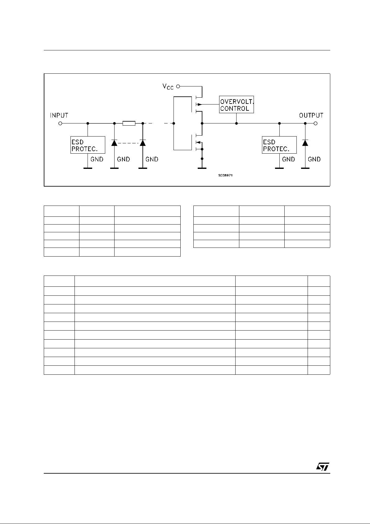
Power down prot ec tion is provided on all inputs
and 0 to 7V can be accepted on inputs with no
regard to the supply voltage. Th is device can be
usedto interface5V to 3V.
This together with its schmitt t rigger function
allows it to be used on line receivers with slow
rise/fall input signals.
All inputs and outputs are equipped with
protection circuits against static discharge.
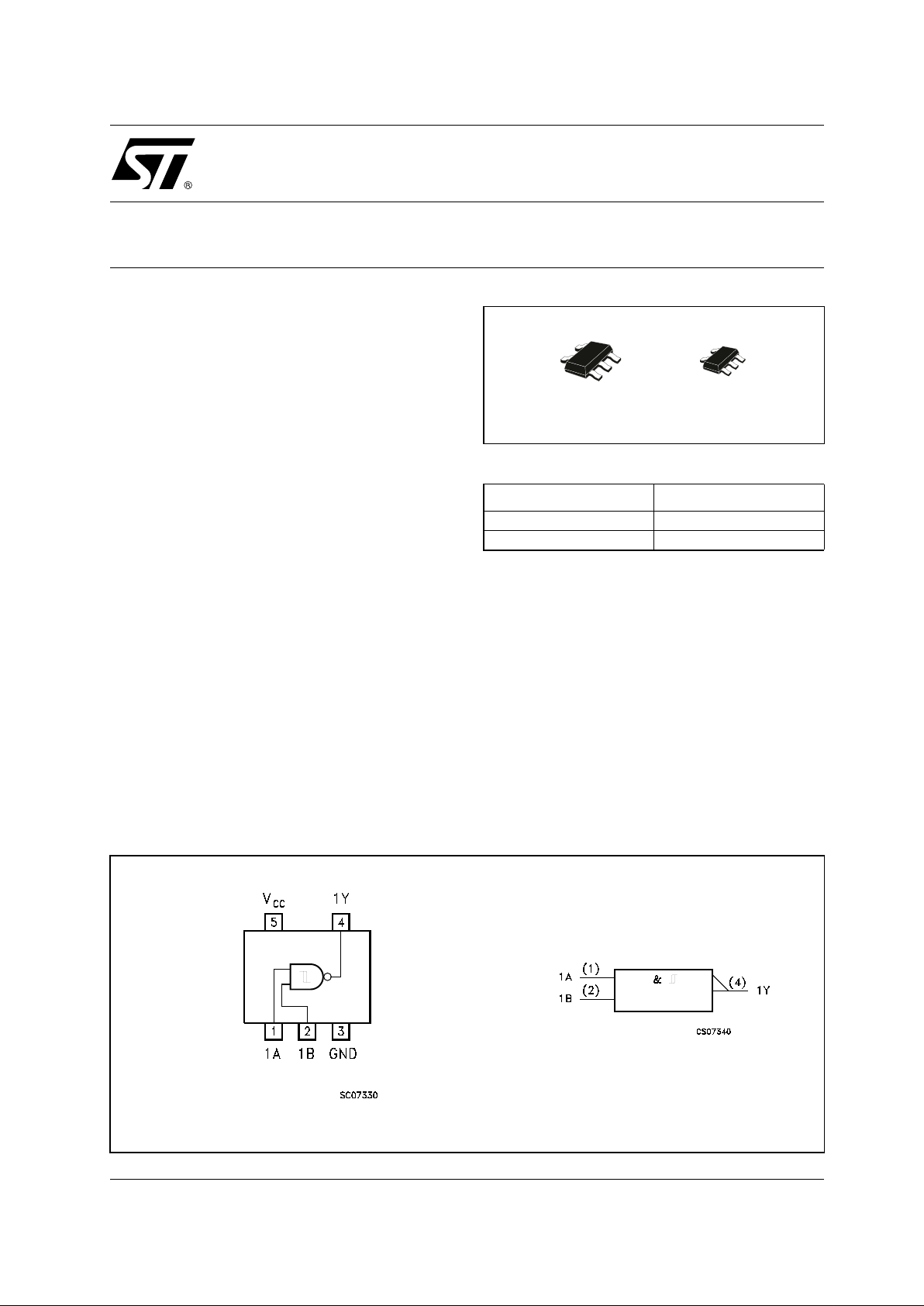
74LX1G132
SINGLE 2-INPUT SCHMITT NAND GATE
PIN CONNECTION AND IEC LOGIC SYMBOLS
ORDER CODES
PACKAGE T & R
SOT23-5L 74LX1G132STR
SOT323-5L 74LX1G132CTR
SOT323-5LSOT23-5L
74LX1G132
2/11
INPUT EQUIVALENT CIRCUIT
PIN DESCRIPTION TRUTH TABLE
ABSOLUTE MAXIMUM RATINGS
Absolute Maximum Ratings are those values beyond which damage to the device may occur. Functional operation under these conditions is
not implied.
1) I
O
maximum rating must be observed
2) V
O
<GND,VO>V
CC
PIN No SYMBOL NAME AND FUNCTION
1 1A Data Input
2 1B Data Input
4 1Y Data Output
3 GND Ground (0V)
5
V
CC
Positive Supply Voltage
ABY
LLH
LHH
HLH
HHL
Symbol Parameter Value Unit
V
CC
Supply Voltage
-0.5 to +7.0 V
V
I
DC Input Voltage
-0.5 to +7.0 V
V
O
DC Output Voltage (VCC= 0V)
-0.5 to +7.0 V
V
O
DC Output Voltage (High or Low State) (note 1) -0.5 to VCC+ 0.5
V
I
IK
DC Input Diode Current
-50 mA
I
OK
DC Output Diode Current (note 2)
-50 mA
I
O
DC Output Current
± 50 mA
I
CC
or I
GND
DC VCCor Ground Current per Supply Pin
± 50 mA
T
stg
Storage Temperature
-65 to +150 °C
T
L
Lead Temperature (10 sec)
300 °C
74LX1G132
3/11
RECOMMENDED OPERATING CONDITIONS
1) Truth Table guaranteed: 1.2V to 3.6V
Symbol Parameter Value Unit
V
CC
Supply Voltage (note 1)
1.65 to 5.5 V
V
I
Input Voltage
0 to 5.5 V
V
O
Output Voltage (VCC= 0V)
0 to 5.5 V
V
O
Output Voltage (High or Low State) 0 to V
CC
V
I
OH,IOL
High or Low Level Output Current (VCC= 4.5 to 5.5V)
± 32 mA
I
OH,IOL
High or Low Level Output Current (VCC= 3.0 to 3.6V)
± 24 mA
I
OH,IOL
High or Low Level Output Current (VCC= 2.7 to 3.0V)
± 12 mA
I
OH,IOL
High or Low Level Output Current (VCC= 2.3 to 2.7V)
± 8mA
I
OH,IOL
High or Low Level Output Current (VCC= 1.65 to 2.3V)
± 4mA
T
op
Operating Temperqture
-55 to 125 °C
74LX1G132
4/11
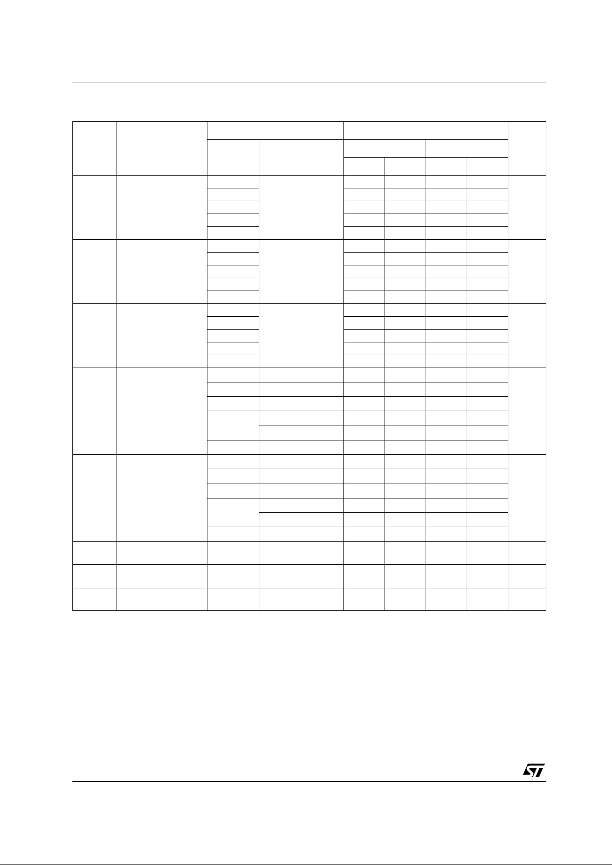
DC SPECIFICATIONS
Symbol Parameter
Test Condition Value
Unit
V
CC
(V)
-40 to 85 °C -55 to 125 °C
Min. Max. Min. Max.
V
T+
Positive Input
threshold
1.65 0.79 1.16 0.79 1.16
V
2.3 1.11 1.56 1.11 1.56
3 1.5 1.87 1.5 1.87
4.5 2.16 2.74 2.16 2.74
5.5 2.61 3.33 2.61 3.33
V
T-
Negative Input
threshold
1.65 0.39 0.62 0.39 0.62
V
2.3 0.58 0.87 0.58 0.87
3 0.84 1.14 0.84 1.14
4.5 1.41 1.79 1.41 1.79
5.5 1.87 2.29 1.87 2.29
V
H
Hysteresis Voltage 1.65 0.37 0.62 0.37 0.62
V
2.3 0.48 0.77 0.48 0.77
3 0.56 0.87 0.56 0.87
4.5 0.71 1.04 0.71 1.04
5.5 0.71 1.11 0.71 1.11
V
OH
High Level Output
Voltage
1.65 to 4.5
IO=-100 µAVCC-0.1 VCC-0.1
V
1.65
I
O
=-4 mA
1.2 1.2
2.3
I
O
=-8 mA
1.9 1.9
3.0
I
O
=-16 mA
2.4 2.4
I
O
=-24 mA
2.2 2.2
4.5
I
O
=-32 mA
3.8 3.8
V
OL
Low Level Output
Voltage
1.65 to 4.5
I
O
=100 µA
0.1 0.1
V
1.65
I
O
=4 mA
0.45 0.45
2.3
I
O
=8 mA
0.3 0.3
3.0
I
O
=16 mA
0.4 0.4
I
O
=24 mA
0.55 0.55
4.5
I
O
=32 mA
0.55 0.55
I
I
Input Leakage
Current
1.65 to 5.5
V
I
= 0 to 5.5V
± 10 ±10 µA
I
off
Power Off Leakage
Current
0
V
I
or VO= 5.5V
10 10 µA
I
CC
Quiescent Supply
Current
1.65 to 5.5
V
I=VCC
or GND
10 10 µA
 Loading...