

SGS Thomson Microelectronics 74LVX74M, 74LVX74TTR, 74LVX74MTR Datasheet
1/11July 2001
■ HIGH SPEED :
f
MAX
= 145MHz (TYP.) at V
CC
= 3.3V
■ 5V TOLERANT INPUTS
■ INPUT VOLTAGE LEVEL :
V
IL
=0.8V , VIH=2V AT VCC=3V
■ LOW POWER DISSIPATION:
I
CC
= 2 µA (MAX.) at TA=25°C
■ LOW NOISE:
V
OLP
= 0.3V (TYP.) at VCC = 3.3V
■ SYMMETRICAL OUTPUT IMPEDANCE:
|I
OH
| = IOL = 4mA (MIN)
■ BALANCED PROPAGATION DELAYS:
t
PLH
≅ t
PHL
■ OPERATING VOL TAGE RANGE:
V
CC
(OPR) = 2V to 3.6V (1.2V Data Retention)
■ PIN AND FUNCTION COMPATIBLE WITH
74 SERIES 74
■ IMPROVED LATCH-UP IMMUNITY
■ POWER DOWN PROTECTION ON INPUTS
DESCRIPTION
The 74LVX74 is a low voltage CMOS DUAL
D-TYPE FLIP-FLOP WITH PRESET AND CLEAR
NON INVERTING fabricated with sub-micron
silicon gate and double-layer metal wiring C
2
MOS
technology. It is ideal for low power, battery
operated and low noise 3.3V applications.
A signal on the D INPUT is transferred to the Q
OUTPUT during the positive going transition of the
clock pulse. CLR
and PR are independent of the
clock and accomplished by a low setting on the
appropriate input.
Power down protection is provided on all inputs
and 0 to 7V can be accepted on inputs with no
regard to the supply voltage.
This device can be used to interface 5V to 3V
system. It combines high speed performance with
the true CMOS low power consumption. All inputs
and outputs are eq uipped with protection circuits
against static discharge, giving them 2KV ESD
immunity and transient excess voltage.
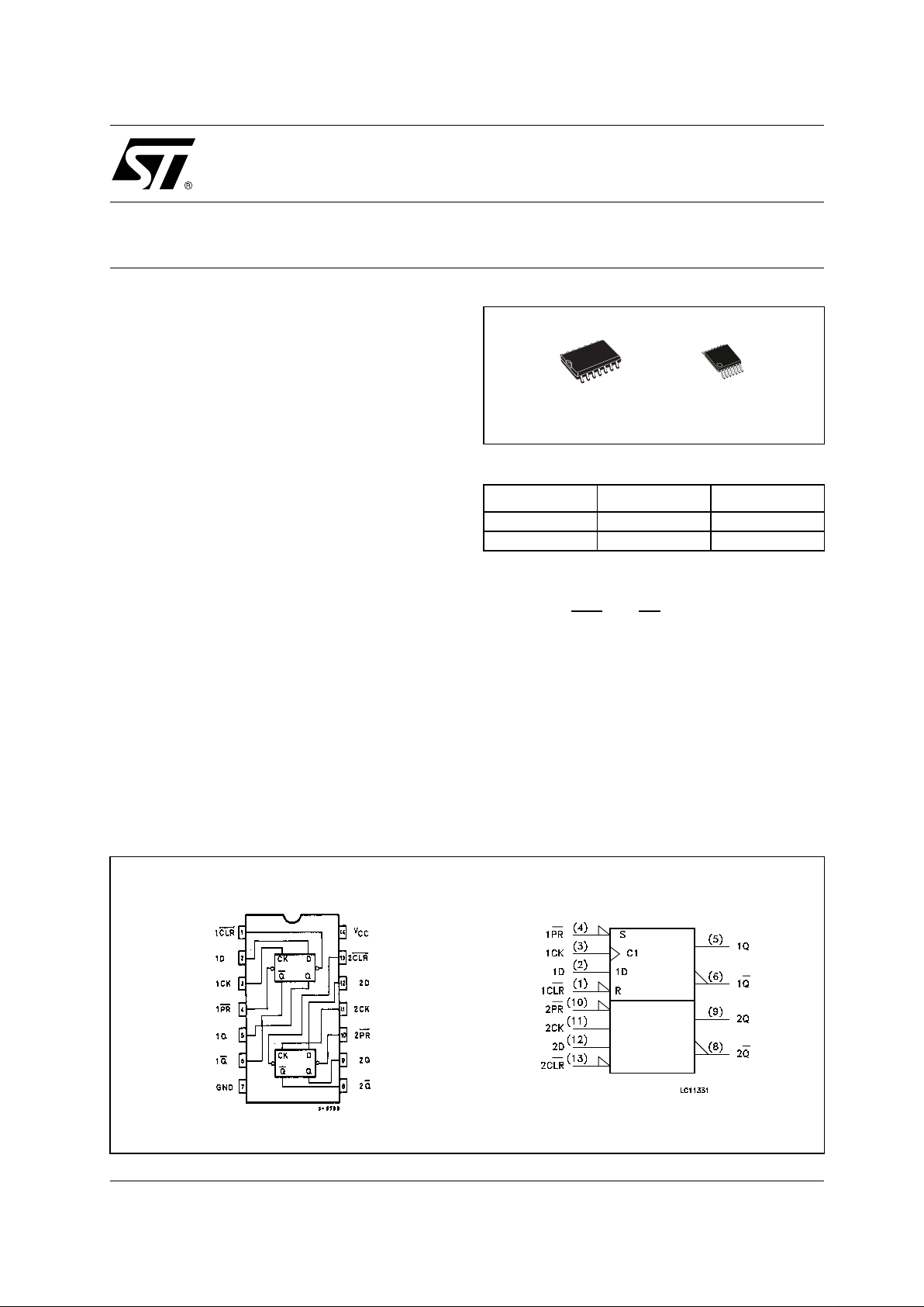
74LVX74
LOW VOLTAGE CMOS DUAL D-TYPE FLIP FLOP
WITH PRESET AND CLEAR (5V TOLERANT INPUTS)
PIN CONNECTION AND IEC LOGIC SYMBOLS
ORDER CODES
PACKAGE TUBE T & R
SOP 74LVX74M 74LVX74MTR
TSSOP 74LVX74TTR
TSSOPSOP
74LVX74
2/11
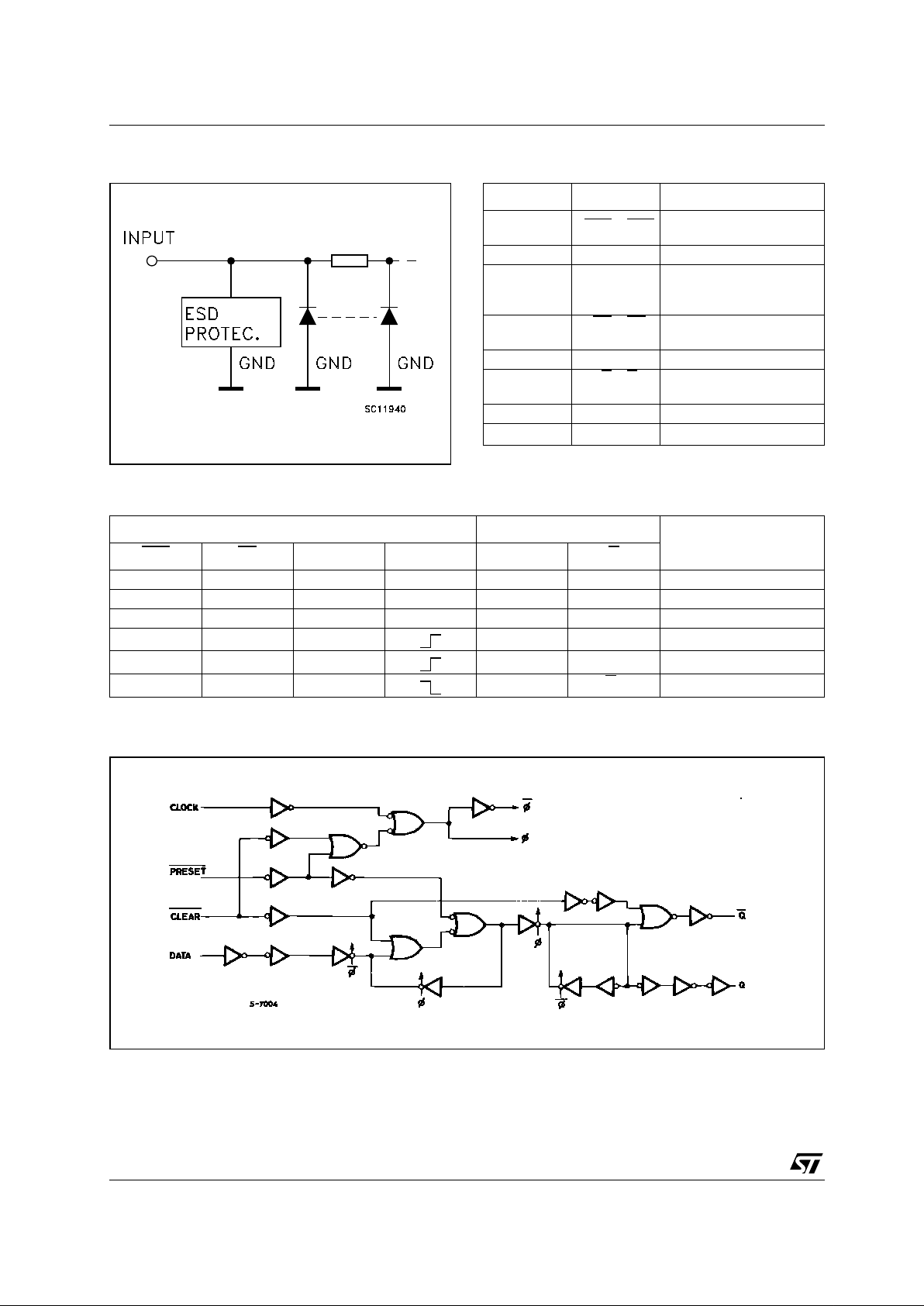
INPUT EQUIVALENT CIRCUIT PIN DESCRIPTION
TRUTH TABLE
X : Don’t Care
LOGIC DIAGRAM
This log i c diagram has not be used to esti m at e propagation delays
PIN No SYMBOL NAME AND FUNCTION
1, 13 1CLR
, 2CLR
Asynchronous Reset -
Direct Input
2, 12 1D, 2D Data Inputs
3, 11 1CK, 2CK Clock Input
(LOW to HIGH, Edge
Triggered)
4, 10 1PR
, 2PR Asynchronous Set - Direct
Input
5, 9 1Q, 2Q True Flip-Flop Outputs
6, 8 1Q
, 2Q Complement Flip-Flop
Outputs
7 GND Ground (0V)
14 V
CC
Positive Supply Voltage
INPUTS OUTPUTS
FUNCTION
CLR
PR DCKQ Q
L H X X L H CLEAR
H L X X H L PRESET
LLXXHH
HHL LH
HHH HL
HHX
Q
n
Q
n
NO CHANGE
74LVX74
3/11
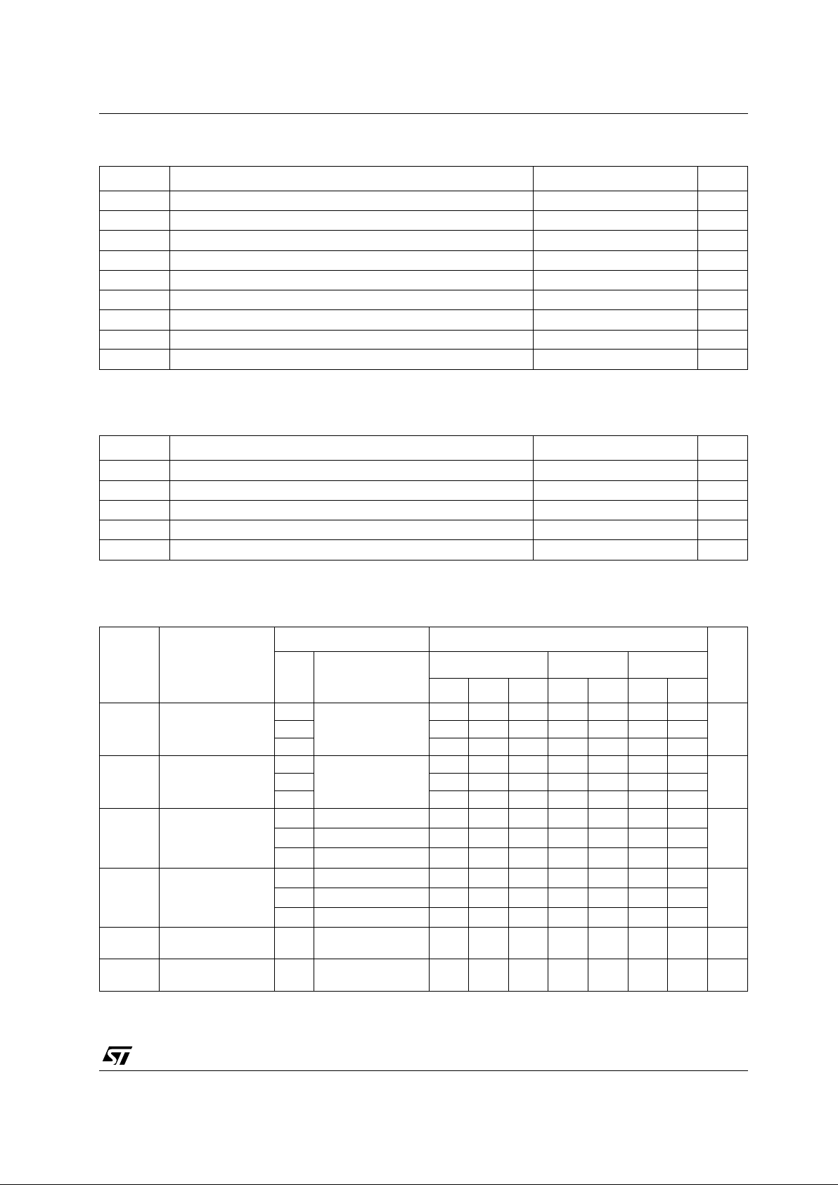
ABSOLUTE MAXIMUM RATINGS
Absolute Maximum Ratings are those values beyond which damage to the device may occur. Functional operation under these conditions is
not implied.
RECOMMENDED OPERATING CONDITIONS
1) Truth T abl e guarante ed: 1.2V to 3.6 V
2) V
IN
from 0.8V to 2.0V
DC SPECIFICATIONS
Symbol Parameter Value Unit
V
CC
Supply Voltage
-0.5 to +7.0 V
V
I
DC Input Voltage
-0.5 to +7.0 V
V
O
DC Output Voltage -0.5 to VCC + 0.5
V
I
IK
DC Input Diode Current
- 20 mA
I
OK
DC Output Diode Current
± 20 mA
I
O
DC Output Current
± 25 mA
I
CC
or I
GND
DC VCC or Ground Current
± 50 mA
T
stg
Storage Temperature
-65 to +150 °C
T
L
Lead Temperature (10 sec)
300 °C
Symbol Parameter Value Unit
V
CC
Supply Voltage (note 1)
2 to 3.6 V
V
I
Input Voltage
0 to 5.5 V
V
O
Output Voltage 0 to V
CC
V
T
op
Operating Temperature
-55 to 125 °C
dt/dv
Input Rise and Fall Time (note 2) (V
CC
= 3.3V)
0 to 100 ns/V
Symbol Parameter
Test Condition Value
Unit
V
CC
(V)
T
A
= 25°C
-40 to 85°C -55 to 125°C
Min. Typ. Max. Min. Max. Min. Max.
V
IH
High Level Input
Voltage
2.0 1.5 1.5 1.5
V3.0 2.0 2.0 2.0
3.6 2.4 2.4 2.4
V
IL
Low Level Input
Voltage
2.0 0.5 0.5 0.5
V3.0 0.8 0.8 0.8
3.6 0.8 0.8 0.8
V
OH
High Level Output
Voltage
2.0
I
O
=-50 µA
1.9 2.0 1.9 1.9
V3.0
I
O
=-50 µA
2.9 3.0 2.9 2.9
3.0
I
O
=-4 mA
2.58 2.48 2.4
V
OL
Low Level Output
Voltage
2.0
I
O
=50 µA
0.0 0.1 0.1 0.1
V3.0
I
O
=50 µA
0.0 0.1 0.1 0.1
3.0
I
O
=4 mA
0.36 0.44 0.55
I
I
Input Leakage
Current
3.6
V
I
= 5V or GND
± 0.1 ± 1 ± 1 µA
I
CC
Quiescent Supply
Current
3.6
V
I
= VCC or GND
22020µA
74LVX74
4/11
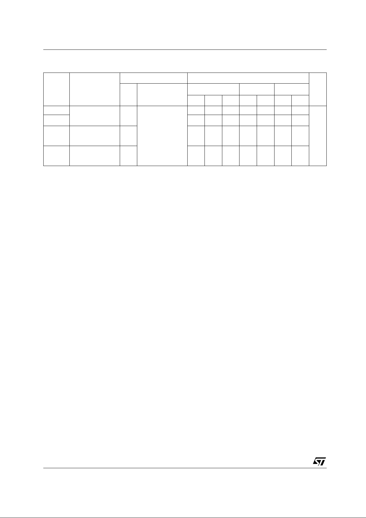
DYNAMIC SWITCHING CHARACTERISTICS
1) Worst c ase package .
2) Max number of outp ut s defined as (n). Data inputs are driven 0V to 3.3V, (n-1) outputs switching and one output at GND.
3) Max number of data inputs (n) switching. (n-1) switching 0V to 3.3V. Inputs under test switching: 3.3V to threshold (V
ILD
), 0V to threshold
(V
IHD
), f=1MHz.
Symbol Parameter
Test Condition Value
Unit
V
CC
(V)
T
A
= 25°C
-40 to 85°C -55 to 125°C
Min. Typ. Max. Min. Max. Min. Max.
V
OLP
Dynamic Low
Voltage Quiet
Output (note 1, 2)
3.3
C
L
= 50 pF
0.3 0.5
V
V
OLV
-0.5 -0.3
V
IHD
Dynamic High
Voltage Input (note
1, 3)
3.3 2
V
ILD
Dynamic Low
Voltage Input (note
1, 3)
3.3 0.8
 Loading...