

1/11January 2003
■ HIGH SPEED :
t
PD
= 5.5ns (TYP.) at VCC=3.3V
■ 5V TOLERANT INPUTS
■ INPUT VOLTAGE LEVEL :
V
IL
=0.8V, VIH=2V at VCC=3V
■ LOW POWER DISSIPATION:
I
CC
=4µA (MAX.) at TA=25°C
■ LOW NOISE:
V
OLP
=0.3V(TYP.)atVCC=3.3V
■ SYMMETRICAL OUTPUT IMPEDANCE:
|I
OH
|=IOL=4mA(MIN)
■ BALANCED PROPAGATION DELAYS:
t
PLH
≅ t
PHL
■ OPERATING VOLTAGE RANGE:
V
CC
(OPR) = 2V to 3.6V (1.2V Data Retention)
■ PIN AND FUNCTION COMPATIBLE WITH
74 SERIES 594
■ IMPROVED LATCH-UP IMMUNITY
■ POWER DOWN PROTECTION ON INPUTS
DESCRIPTION
The 74LVX594 is a low voltage CMOS 8 BIT
SHIFT REGISTER WITH OUTPUT REGISTER
fabricated with sub-micron silicon gate and
double-layer metal wiring C
2
MOS technology. It is
ideal for low power, battery operated and low
noise 3.3V applications.
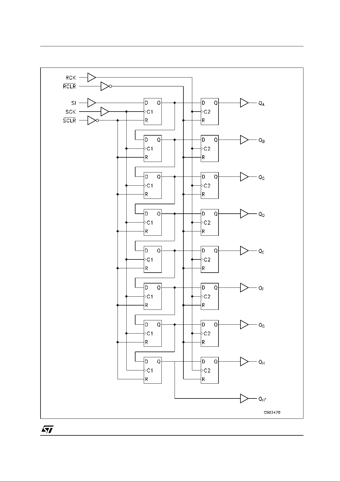
This device contains an 8-bit serial-in, parallel-out
shift register that feeds an 8-bit D-type storage
register. Separate clocks an d direct overriding
clear(SCLR,
RCLR) are provided for bot h the shift
register and the storage register. A serial (QH’)
output is provided for cascading purposes. Both
the shift register and sto rage register use
positive-edge triggered clocks. If the clocks are
connected together, the shift register state will
always be one clock pulse ahead of the storage
register.
Power down protection is provided on all inputs
and 0 to 7V can be accepted on inputs with no
regard to the supply voltage. This device can be
used to interface 5V to 3V system. It combines
high s peed performance with the true CMOS low
power consumption.
All inputs and outputs are equipped with
protection circuits against s tatic discharge, giving
them 2K V ESD immunity and t ransient excess
voltage.
74LVX594
LOW VOLTAGE CMOS 8 BIT SHIFT REGISTER
WITH OUTPUT REGISTER (5V TOLERANT INPUTS)
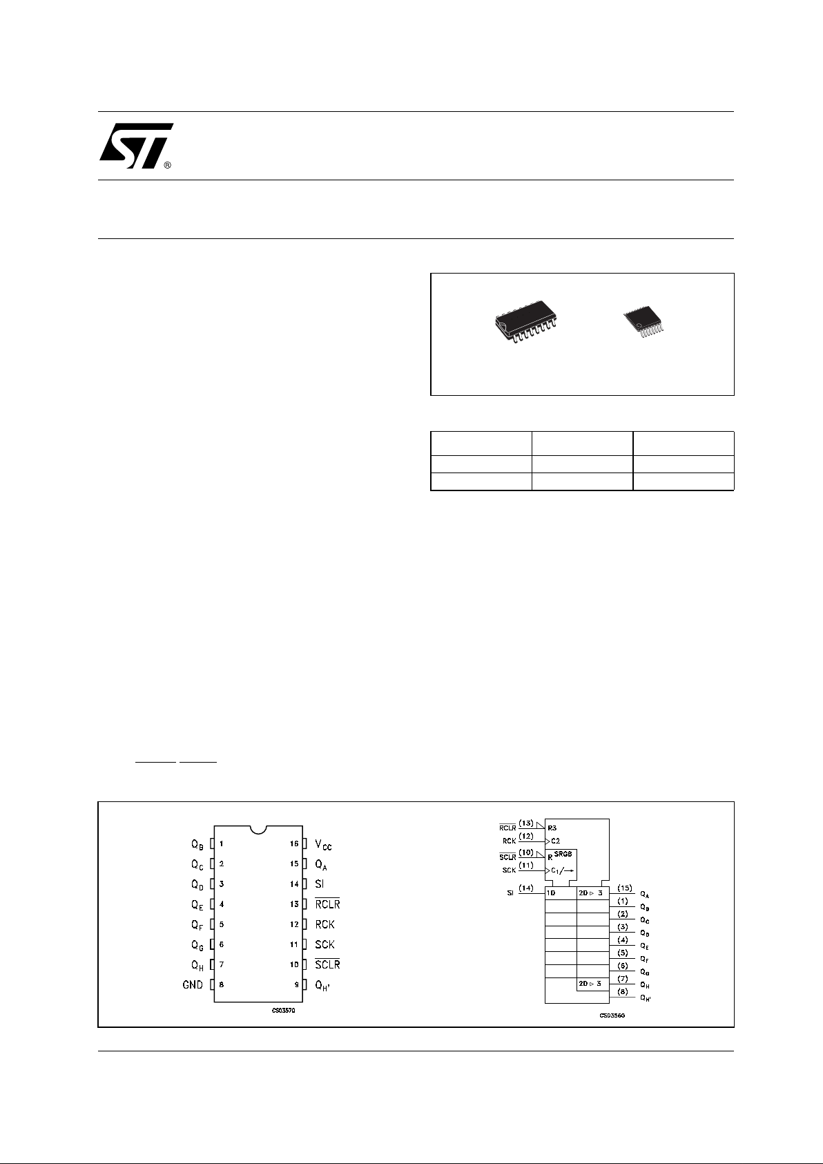
PIN CONNECTION AND IEC LOGIC SYMBOLS
ORDER CODES
PACKAGE TUBE T & R
SOP 74LVX594M 74LVX594MTR
TSSOP 74LVX594TTR
TSSOPSOP
74LVX594
2/11
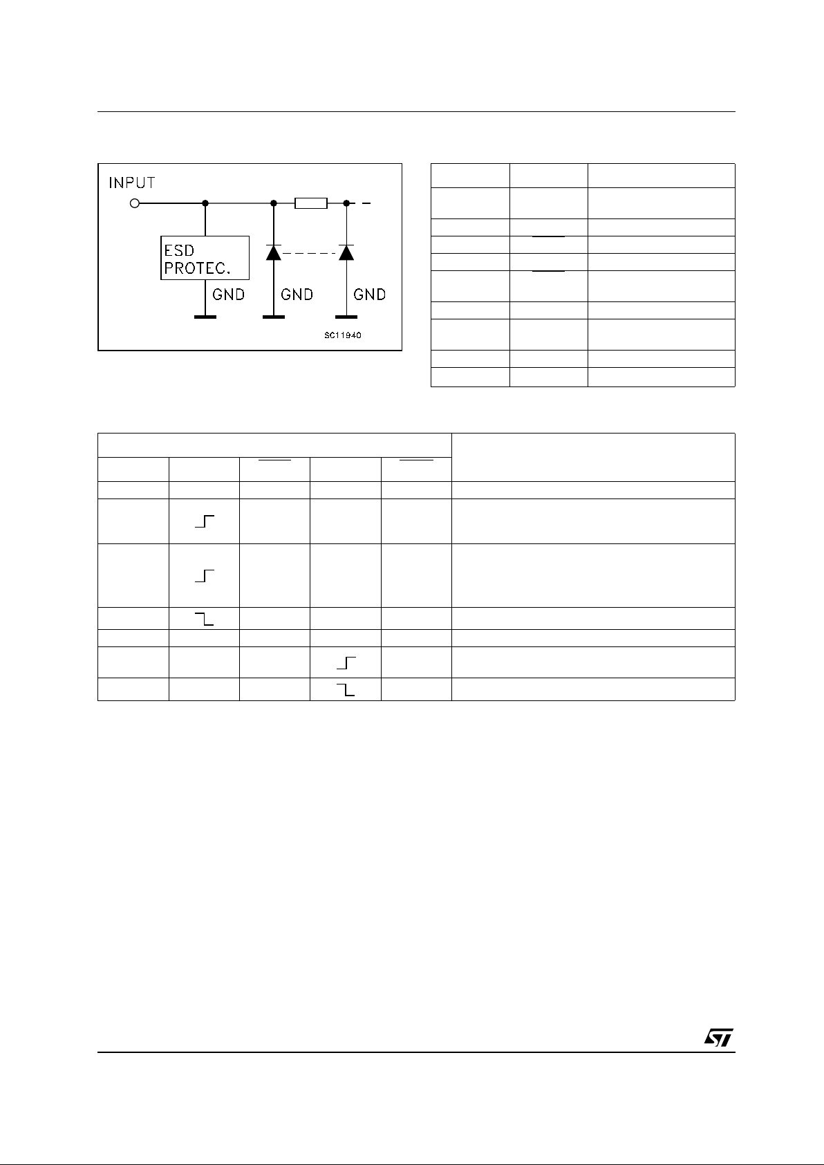
INPUT EQ UIVALENT CIRCUIT PIN DESCRIPTION
TRUTH TABLE
X : Don’t Care
PIN No SYMBOL NAME AND FUNCTION
1, 2, 3, 4,5,
6, 7, 15
QA to QH Data Outputs
9 QH’ Serial Data Output
10 SCLR
Shift Register Clear Input
11 SCK Shift Register Clock Input
13 RCLR
Storage Register Clear
Input
14 SI Serial Data Input
12 RCK Storage Register Clock
Input
8 GND Ground (0V)
16 V
CC
Positive Supply Voltage
INPUTS
OUTPUTS
SI SCK SCLR RCK RCLR
X X L X X SHIFT REGISTER IS CLEAR
LHXX
FIRST STAGE OF SHIFT REGISTER GOES LOW
OTHER STAGES STORE THE DATA OF PREVI-
OUS STAGE, RESPECTIVELY
HHXX
FIRST STAGE OF SHIFT REGISTER GOES HIGH
OTHER STAGES STORE THE DATA OF PREVI-
OUS STAGE, RESPECTIVELY
L H X X SHIFT REGISTER STATEIS NOT CHANGED
X X X X L STORAGE REGISTER IS CLEARED
XXX H
SHIFT REGISTER DATAIS STORED IN THE
STORAGE REGISTER
X X X H STORAGE REGISTER STATE IS NOT CHANGED
74LVX594
3/11
LOGIC DIAGRAM
This logic diagram has not be used to estimate propagation delays
74LVX594
4/11
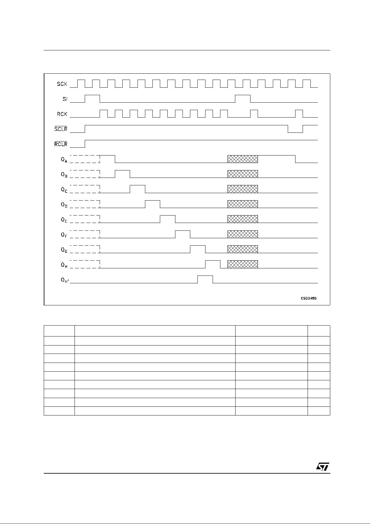
TIMING CHART
ABSOLUTE MAXIMUM RATINGS
Absolute Maximum Ratings are those values beyond which damage to the device may occur. Functional operation under these conditions is
not implied.
Symbol Parameter Value Unit
V
CC
Supply Voltage
-0.5 to +7.0 V
V
I
DC Input Voltage
-0.5 to +7.0 V
V
O
DC Output Voltage -0.5 to VCC+ 0.5
V
I
IK
DC Input Diode Current
-20 mA
I
OK
DC Output Diode Current
± 20 mA
I
O
DC Output Current
± 25 mA
I
CC
or I
GND
DC VCCor Ground Current
± 50 mA
T
stg
Storage Temperature
-65 to +150 °C
T
L
Lead Temperature (10 sec)
300 °C

74LVX594
5/11
RECOMMENDED OPERATING CONDITIONS
1) Truth Table guaranteed: 1.2V to 3.6V
2) V
IN
from0.8Vto 2.0V
DC SPECIFICATIONS
DYNAMIC SWITCH ING CHARACTERISTICS
1) Worst case package.
2) Max number of outputs defined as (n). Data inputs are driven 0V to 3.3V, (n-1) outputs switching and one output at GND.
3) Max number of data inputs (n) switching. (n-1) switching 0V to 3.3V. Inputs under test switching: 3.3V to threshold (V
ILD
), 0V to threshold
(V
IHD
), f=1MHz.
Symbol Parameter Value Unit
V
CC
Supply Voltage (note 1)
2 to 3.6 V
V
I
Input Voltage
0 to 5.5 V
V
O
Output Voltage 0 to V
CC
V
T
op
Operating Temperature
-55 to 125 °C
dt/dv
Input Rise and Fall Time (note 2) (V
CC
= 3.3V)
0 to 100 ns/V
Symbol Parameter
Test Condition Value
Unit
V
CC
(V)
T
A
= 25°C
-40 to 85°C -55 to 125°C
Min. Typ. Max. Min. Max. Min. Max.
V
IH
High Level Input
Voltage
2.0 1.5 1.5 1.5
V3.0 2.0 2.0 2.0
3.6 2.4 2.4 2.4
V
IL
Low Level Input
Voltage
2.0 0.5 0.5 0.5
V3.0 0.8 0.8 0.8
3.6 0.8 0.8 0.8
V
OH
High Level Output
Voltage
2.0
I
O
=-50 µA
1.9 2.0 1.9 1.9
V3.0
I
O
=-50 µA
2.9 3.0 2.9 2.9
3.0
I
O
=-4 mA
2.58 2.48 2.4
V
OL
Low Level Output
Voltage
2.0
IO=50 µA
0.0 0.1 0.1 0.1
V3.0
I
O
=50 µA
0.0 0.1 0.1 0.1
3.0
I
O
=4 mA
0.36 0.44 0.55
I
I
Input Leakage
Current
3.6
V
I
=5VorGND
±0.1 ± 1 ± 1 µA
I
off
Power Off Leakage
Current
0
V
I
= 0 to 5V
± 0.1 ± 5 ± 5 µA
I
CC
Quiescent Supply
Current
3.6
V
I=VCC
or GND
44040µA
Symbol Parameter
Test Condition Value
Unit
V
CC
(V)
T
A
= 25°C
-40 to 85°C -55 to 125°C
Min. Typ. Max. Min. Max. Min. Max.
V
OLP
Dynamic Low Voltage
Quiet Output (note 1, 2)
3.3
C
L
=50pF
0.3 0.5
V
V
OLV
-0.5 -0.3
V
IHD
Dynamic High Voltage
Input (note 1, 3)
3.3 2
V
ILD
Dynamic Low Voltage
Input (note 1, 3)
3.3 0.8

74LVX594
6/11
AC E LECTRICAL CHARACTERISTICS (Input tr=tf=3ns)
1) Skew is defined as the absolute value of the difference between the actual propagation delay for any two outputs of the same device switching in the same direction, either HIGH or LOW
2) Parameter guaranteed by design
(*) Voltagerange is 3.3V± 0.3V
Symbol Parameter
Test Condition Value
Unit
V
CC
(V)
C
L
(pF)
T
A
= 25°C
-40 to 85°C -55 to 125°C
Min. Typ. Max. Min. Max. Min. Max.
t
PLHtPHL
Propagation Delay
Time
(RCK - Qn)
2.7 15 5.5 9.5 1.0 10.0 1.0 10.0
ns
2.7 50 9.0 13.0 1.0 14.5 1.0 14.5
3.3
(*)
15 4.9 8.2 1.0 8.8 1.0 8.8
3.3
(*)
50 8.1 11.9 1.0 13.1 1.0 13.1
t
PLHtPHL
Propagation Delay
Time
(SCK - QH’)
2.7 15 6.5 11.0 1.0 12.5 1.0 12.5
ns
2.7 50 9.2 14.0 1.0 16.0 1.0 16.0
3.3
(*)
15 5.5 9.2 1.0 9.9 1.0 9.9
3.3
(*)
50 8.4 12.5 1.0 13.9 1.0 13.9
t
PHL
Propagation Delay
Time
(RCLR
- Qn)
2.7 15 7.3 11.0 1.0 13.0 1.0 13.0
ns
2.7 50 10.5 14.5 1.0 16.0 1.0 16.0
3.3
(*)
15 6.0 9.8 1.0 10.6 1.0 10.6
3.3
(*)
50 9.0 13.1 1.0 14.4 1.0 14.4
t
PLHtPHL
Propagation Delay
Time
(SCLR
- QH’)
2.7 15 6.3 10.5 1.0 12.0 1.0 12.0
ns
2.7 50 9.0 13.5 1.0 15.5 1.0 15.5
3.3
(*)
15 5.6 9.2 1.0 10.0 1.0 10.0
3.3
(*)
50 8.5 12.4 1.0 14.0 1.0 14.0
f
MAX
Maximum Clock
Frequency
2.7 15 70 110 60 60
MHz
2.7 50 40 90 35 35
3.3
(*)
15 80 120 70 70
3.3
(*)
50 55 105 50 50
t
W(H)
Minimum Pulse
Width (SCK, RCK)
2.7 50 6.5 6.5 6.5
ns
3.3
(*)
50 5.5 5.5 5.5
t
W(L)
Minimum Pulse
Width
(SCLR
,RCLR)
2.7 50 5.0 5.0 5.0
ns
3.3
(*)
50 5.0 5.0 5.0
t
s
Minimum Set-Up
Time (SI - CCK)
2.7 50 3.5 3.5 3.5
ns
3.3
(*)
50 3.0 3.0 3.0
t
s
Minimum Set - Up
Time (SCK, RCK)
2.7 50 9.0 9.0 9.0
ns
3.3
(*)
50 85. 8.5 8.5
t
s
Minimum Set - Up
Time (SCRL
- RCK)
2.7 50 8.0 8.0 8.0
ns
3.3
(*)
50 7.5 7.5 7.5
t
h
Minimum Hold
Time
2.7 50 1.5 1.5 1.5
ns
3.3
(*)
50 1.5 1.5 1.5
t
REM
Minimum ClearRemoval Time
2.7 50 3.0 3.0 3.0
ns
3.3
(*)
50 3.0 3.0 3.0
t
OSLH
t
OSHL
Output To Output
Skew Time (note1,
2)
2.7 50 0.5 1.0 1.5 1.5
ns
3.3
(*)
50
0.5 1.0 1.5 1.5

74LVX594
7/11
CAPACITIVE CHARACTERISTICS
1) CPDis defined as the value of the IC’s internal equivalent capacitance which is calculated from the operating current consumption without
load. (Refer to Test Circuit). Average operating current can be obtained by the following equation. I
CC(opr)=CPDxVCCxfIN+ICC
TEST CIRCUIT
CL=15/50pF or equivalent (includes jig and probe capacitance)
R
T=ZOUT
of pulse generator (typically 50Ω)
Symbol Parameter
Test Condition Value
Unit
V
CC
(V)
T
A
= 25°C
-40 to 85°C -55 to 125°C
Min. Typ. Max. Min. Max. Min. Max.
C
IN
Input Capacitance
3.3 7 10 10 10 pF
C
OUT
Output
Capacitance
3.3 9 pF
C
PD
Power Dissipation
Capacitance
(note 1)
3.3
f
IN
= 10MHz
55 pF

74LVX594
8/11
WAVEFORM 1 : PR OPAGATION DELAYS, SETUP AND HOLD TIMES (f=1MHz; 50% du ty cycle)
WAVEFORM 2: MINIMUM PULSE WIDTH (f=1MHz; 50% duty cycle)

74LVX594
9/11
DIM.
mm. inch
MIN. TYP MAX. MIN. TYP. MAX.
A 1.75 0.068
a1 0.1 0.2 0.004 0.008
a2 1.65 0.064
b 0.35 0.46 0.013 0.018
b1 0.19 0.25 0.007 0.010
C 0.5 0.019
c1 45˚ (typ.)
D 9.8 10 0.385 0. 393
E 5.8 6.2 0.228 0.244
e 1.27 0.050
e3 8.89 0.350
F 3.8 4.0 0. 149 0.157
G 4.6 5.3 0.181 0.208
L 0.5 1.27 0.019 0. 050
M 0.62 0.024
S8 ˚ (max.)
SO-16 MECHANICAL DATA
PO13H

74LVX594
10/11
DIM.
mm. inch
MIN. TYP MAX. MIN. TYP. MAX.
A 1.2 0.047
A1 0.05 0.15 0.002 0.004 0.006
A2 0.8 1 1.05 0.031 0.039 0.041
b 0.19 0.30 0.007 0.012
c 0.09 0.20 0.004 0.0079
D 4.9 5 5.1 0.193 0.197 0.201
E 6.2 6.4 6.6 0.244 0.252 0.260
E1 4.3 4.4 4.48 0.169 0.173 0.176
e 0.65 BSC 0.0256 BSC
K0˚ 8˚0˚ 8˚
L 0.45 0.60 0.75 0.018 0.024 0.030
TSSOP16 MECHANICAL DATA
c
E
b
A2
A
E1
D
1
PIN 1 IDENTIFICATION
A1
L
K
e
0080338D

74LVX594
11/11
Information furnished is believed to be accurate and reliable. However, STMicroelectronics assumes no responsibility for the
consequences of use o f suc h inf ormat ion n or f or an y infr ingeme nt of paten ts or oth er ri gh ts of third part ies whic h may resul t f rom
its use. No license is granted by implication or otherwise under any patent or patent rights of STMicroelectronics. Specifications
mentioned in this publication are subject to change without notice. This publication supersedes and replaces all information
previously supplied. STMicroelectronics products are not authorized for use as critical components in life support devices or
systems without express written approval of STMicroelectronics.
© The ST logo is a registered trademark of STMicroelectronics
© 2003 STMicroelectronics - Printed in Italy - All Rights Reserved
STMicroelectronics GROUP OF COMPANIES
Australia - Brazil - Canada - China - Finland - France - Germany - Hong Kong - India - Israel - Italy - Japan - Malaysia - Malta - Morocco
Singapore - Spain - Sweden - Switzerland - United Kingdom - United States.
© http://www.st.com
 Loading...