

SGS Thomson Microelectronics 74LVX373TTR, 74LVX373MTR, 74LVX373M Datasheet
74LVX373
LOW VOLTAGE CMOS OCTAL D-TYPE LATCH
(3-STATE NON INV.) WITH 5V TOLERANT INPUTS
■ HIGH SPEED:
t
=5.8ns (TYP.) at VCC = 3.3V
PD
■ 5V TOLERANT INPUTS
■ POWER-DOWN PROTECTION ON INPUTS
■ INPUT VOLTAGE LEVEL:
V
= 0.8V, VIH = 2V at VCC =3V
IL
■ LOW POWER DISSIPATION:
I
= 4 µA (MAX.) at TA=25°C
CC
■ LOW NOISE:
V
= 0.3V (TYP.) at VCC =3.3V
OLP
■ SYMMETRICAL OUTPUT IMPEDANCE:
|I
| = IOL = 4 mA (MIN) at VCC =3V
OH
■ BALANCED PROPAGATION DELAYS:
t
≅ t
PLH
■ OPERATING VOLTAGE R ANGE:
V
CC
■ PIN AND FUNCTION COMPATIBLE WITH
PHL
(OPR) = 2V to 3.6V (1.2V Data Retention)
74 SERIES 373
■ IMPROVED LATCH-UP IMMUNITY
DESCRIPTION
The 74LVX373 is a low voltage CMOS OCTAL
D-TYPE LATCH with 3 STATE OUTPUT NON
INVERTING fabricated with sub-micron silicon
gate and double-layer metal wiring C
2
MOS
technology. It is ideal for low power, battery
operated and low noise 3.3V applications.
This 8 bit D-Type latch is controlled by a latch
enable input (LE) and an output enable input (OE
While the LE in put is held at a high level, the Q
outpu ts w ill f ollo w t he da ta input precisely .
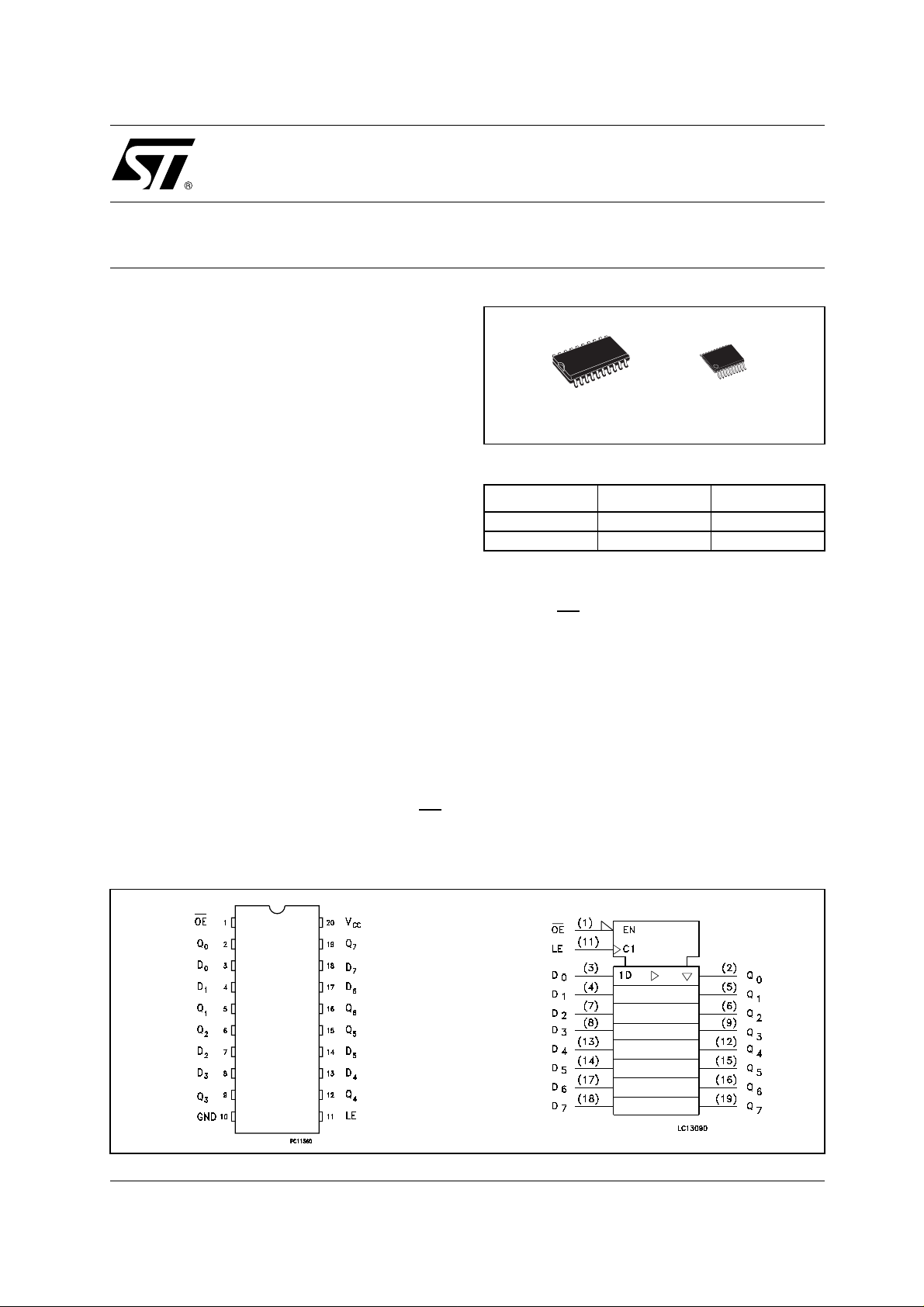
PIN CONNECTION AND IEC LOGIC SYMBOLS
TSSOPSOP
ORDER CODES
PACKAGE TUBE T & R
SOP 74LVX373M 74LVX373MTR
TSSOP 74LVX373TTR
When the LE i s taken low, the Q outputs will be
latched precisely at the logic level of D input data.
While the (OE
) input is low, the 8 outputs will be in
a normal logic state (high or low logic level) and
while high level the outputs will be in a high
impedance state.
Power down protection is provided on all inputs
and 0 to 7V can be accepted on inputs with no
regard to the supply voltage.
This device can be used to interface 5V to 3V. It
combines high speed performance with the true
CMOS low power consumption.
All inputs and outputs are equipped with
protection circuits against stat ic discharge, giving
).
them 2KV ESD immunity and transient excess
voltage.
1/10July 2001
74LVX373
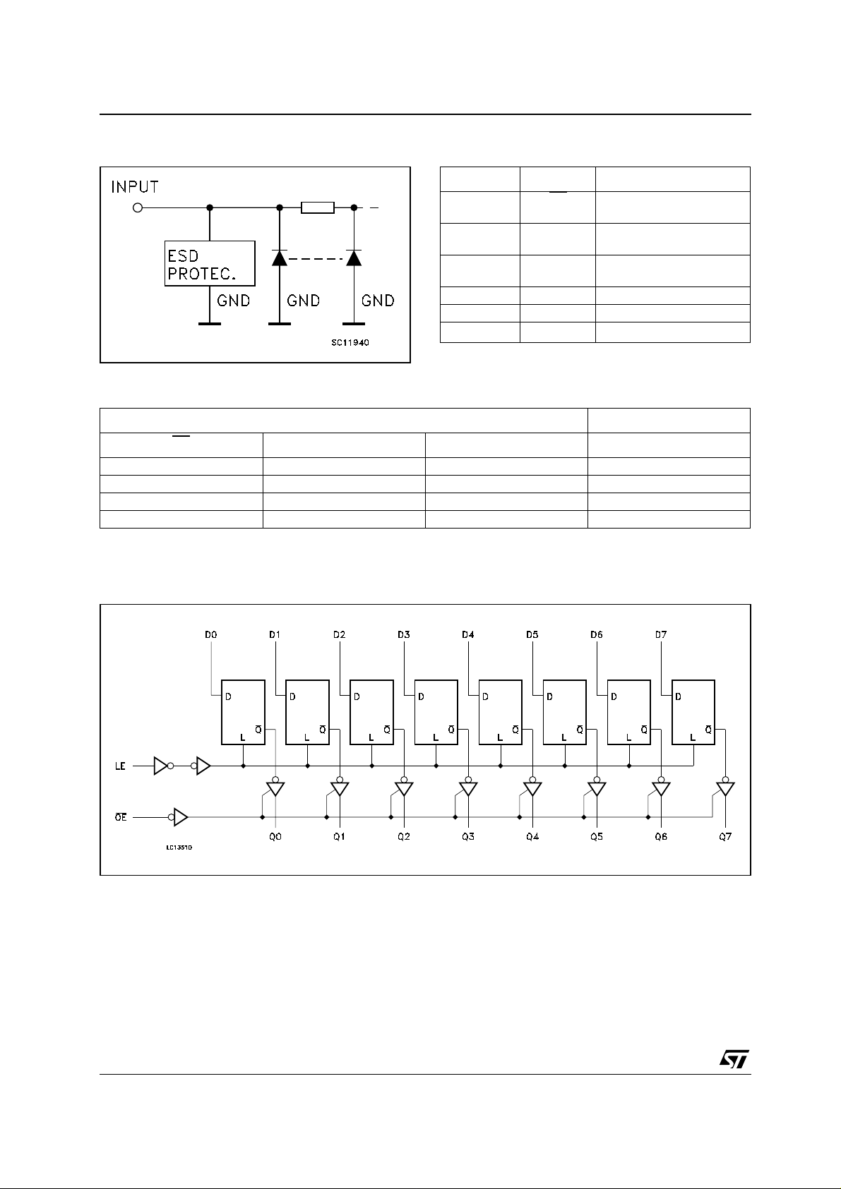
INPUT EQUIVALENT CIRCUIT PIN DESCRIPTION
PIN No SYMBOL NAME AND FUNCTION
1OE
3, 4, 7, 8, 13,
14, 17, 18
2, 5, 6, 9, 12,
15, 16,19
11 LE Latch Enable Input
10 GND Ground (0V)
20 V
TRUTH TABLE
INPUTS OUTPUT
D0 to D7 Data Inputs
Q0 to Q7 3-State Outputs
CC
3 State Output Enable
Input (Active LOW)
Positive Supply Voltage
OE
LE D Q
HXXZ
L L X NO CHANGE*
LHLL
LHHH
X : Don’t Care
Z : High Impedance
* : Q Outputs are Latched at the time when the LE INPUT is taken low logic level
LOGIC DIAGRAM
This log i c diagram has not be used to estimat e propagation del ays
2/10
74LVX373
ABSOLUTE MAXIMUM RATINGS
Symbol Parameter Value Unit
V
V
V
I
I
OK
I
I
or I
CC
T
T
Absolute Maximum Ratings are those values beyond which damage to the device may occur. Functional operation under these conditions is
not implied
RECOMMENDED OPERATING CONDITIONS
Symbol Parameter Value Unit
V
V
V
T
dt/dv
1) Truth T abl e guaranteed: 1.2V to 3.6V
2) V
from 0.8V to 2.0V
IN
Supply Voltage
CC
DC Input Voltage
I
DC Output Voltage -0.5 to VCC + 0.5
O
DC Input Diode Current
IK
DC Output Diode Current
DC Output Current
O
DC VCC or Ground Current
GND
Storage Temperature
stg
Lead Temperature (10 sec)
L
Supply Voltage (note 1)
CC
Input Voltage
I
Output Voltage 0 to V
O
Operating Temperature
op
Input Rise and Fall Time (note 2) (V
CC
= 3V)
-0.5 to +7.0 V
-0.5 to +7.0 V
- 20 mA
± 20 mA
± 25 mA
± 50 mA
-65 to +150 °C
300 °C
2 to 3.6 V
0 to 5.5 V
CC
-55 to 125 °C
0 to 100 ns/V
V
V
DC SPECIFICATIONS
Symbol Parameter
V
V
V
V
I
I
High Level Input
IH
Voltage
Low Level Input
IL
Voltage
High Level Output
OH
Voltage
Low Level Output
OL
Voltage
High Impedance
OZ
Output Leakage
Current
I
Input Leakage
I
Current
Quiescent Supply
CC
Current
Test Condition Value
V
(V)
CC
= 25°C
A
Min. Typ. Max. Min. Max. Min. Max.
-40 to 85°C -55 to 125°C
T
2.0 1.5 1.5 1.5
2.0 2.0 2.0
3.6
2.4 2.4 2.4
2.0 0.5 0.5 0.5
3.6 0.8 0.8 0.8
2.0
3.0
2.0
3.0
3.6
3.6
3.6
IO=-50 µA
I
=-50 µA
O
I
=-4 mA
O
IO=50 µA
I
=50 µA
O
I
=4 mA
O
= VIH or V
V
I
IL
VO = VCC or GND
= 5V or GND
V
I
= VCC or GND
V
I
1.9 2.0 1.9 1.9
2.9 3.0 2.9 2.9
2.58 2.48 2.4
0.0 0.1 0.1 0.1
0.0 0.1 0.1 0.1
0.36 0.44 0.55
±0.25 ± 2.5 ± 5 µA
± 0.1 ± 1 ± 1 µA
44040µA
Unit
V3.0
V3.0 0.8 0.8 0.8
V3.0
V3.0
3/10
 Loading...