

SGS Thomson Microelectronics 74LVX273TTR, 74LVX273MTR, 74LVX273M Datasheet
1/10July 2001
■ HIGH SPEED:
f
MAX
= 150 MHz (TYP.) at VCC = 3.3V
■ 5V TOLERANT INPUTS
■ POWER-DOWN PROTECTION ON INPUTS
■ INPUT VOLTAGE LEVEL:
V
IL
= 0.8V, VIH = 2V at VCC =3V
■ LOW POWER DISSIPATION:
I
CC
= 4 µA (MAX.) at TA=25°C
■ LOW NOISE:
V
OLP
= 0.3V (TYP.) at VCC =3.3V
■ SYMMETRICAL OUTPUT IMPEDANCE:
|I
OH
| = IOL = 4 mA (MIN) at VCC =3V
■ BALANCED PROPAGATION DELAYS:
t
PLH
≅ t
PHL
■ OPERATING VOLT AG E R ANGE:
V
CC
(OPR) = 2V to 3.6V (1.2V Data Retention)
■ PIN AND FUNCTION COMPATIBLE WITH
74 SERIES 273
■ IMPROVED LATCH-UP IMMUNITY
DESCRIPTION
The 74LVX273 is a low voltage CMOS OCTAL
D-TYPE FLIP-FLOP WITH CLEAR fabricated with
sub-micron silicon gate and double-layer metal
wiring C
2
MOS technology. It is ideal for low
power, battery operated and low noise 3.3V
applications.
Information signals applied to D inputs are
transferred to the Q o utputs on the positive going
edge of the clock pulse.
When the CLE AR
input is held low, the Q outputs
are held low independently of the other inputs.
Power down protection is provided on all inputs
and 0 to 7V can be accepted on inputs with no
regard to the supply voltage.
This device can be used to interface 5V to 3V. It
combines high speed performance with the true
CMOS low power consumption.
All inputs and outputs are equipped with
protection circuits against stat ic discharge, giving
them 2KV ESD immunity and transient excess
voltage.
74LVX273
LOW VOLTAGE CMOS OCTAL D-TYPE FLIP-FLOP
WITH CLEAR (5V TOLERANT INPUTS)
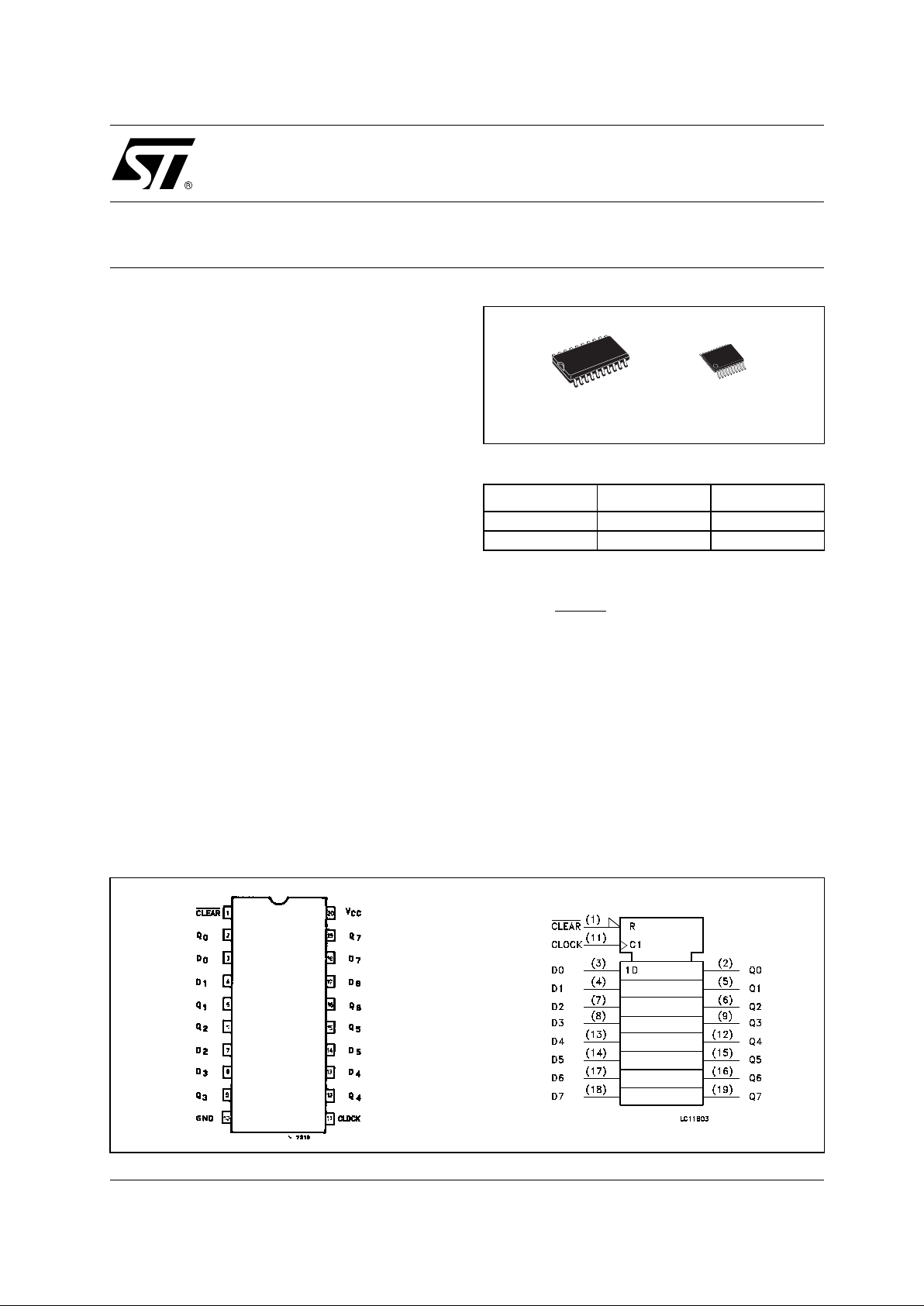
PIN CONNECTION AND IEC LOGIC SYMBOLS
ORDER CODES
PACKAGE TUBE T & R
SOP 74LVX273M 74LVX273MTR
TSSOP 74LVX273TTR
TSSOPSOP
74LVX273
2/10
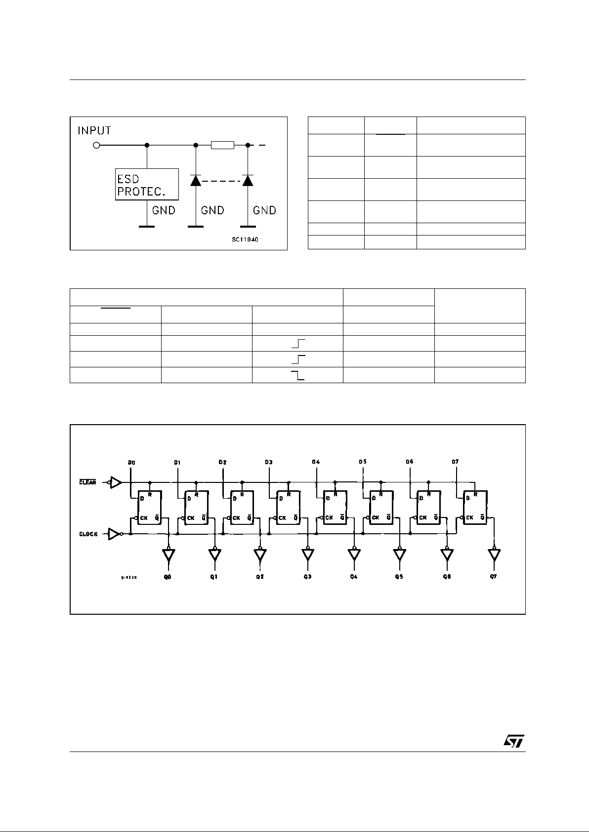
INPUT EQUIVALENT CIRCUIT PIN DESCRIPTION
TRUTH TABLE
X : Don’t Care
LOGIC DIAGRAM
This log i c diagram has not be used to esti m ate propagation delays
PIN No SYMBOL NAME AND FUNCTION
1 CLEAR
Asynchronous Master
Reset (Active LOW)
2, 5, 6, 9, 12,
15, 16,19
Q0 to Q7 Flip-Flop Outputs
3, 4, 7, 8, 13,
14, 17, 18
D0 to D7 Data Inputs
1 1 CLOCK Clock Input (LOW-to-HIGH
Edge Triggered)
10 GND Ground (0V)
20 V
CC
Positive Supply Voltage
INPUTS OUTPUT
FUNCTION
CLEAR
DBQ
L X X L CLEAR
HL L
HH H
HX
Q
n
NO CHANGE
74LVX273
3/10
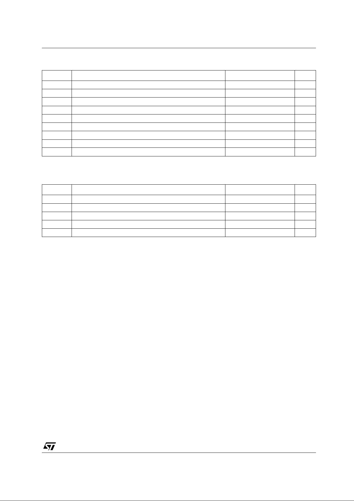
ABSOLUTE MAXIMUM RATINGS
Absolute Maximum Ratings are those values beyond which damage to the device may occur. Functional operation under these conditions is
not implied
RECOMMENDED OPERATING CONDITIONS
1) Truth T abl e guarante ed: 1.2V to 3.6 V
2) V
IN
from 0.8V to 2.0V
Symbol Parameter Value Unit
V
CC
Supply Voltage
-0.5 to +7.0 V
V
I
DC Input Voltage
-0.5 to +7.0 V
V
O
DC Output Voltage -0.5 to VCC + 0.5
V
I
IK
DC Input Diode Current
- 20 mA
I
OK
DC Output Diode Current
± 20 mA
I
O
DC Output Current
± 25 mA
I
CC
or I
GND
DC VCC or Ground Current
± 50 mA
T
stg
Storage Temperature
-65 to +150 °C
T
L
Lead Temperature (10 sec)
300 °C
Symbol Parameter Value Unit
V
CC
Supply Voltage (note 1)
2 to 3.6 V
V
I
Input Voltage
0 to 5.5 V
V
O
Output Voltage 0 to V
CC
V
T
op
Operating Temperature
-55 to 125 °C
dt/dv
Input Rise and Fall Time (note 2) (V
CC
= 3V)
0 to 100 ns/V
 Loading...