

SGS Thomson Microelectronics 74LVX16373TTR Datasheet
74LVX16373
LOW VOLTAGE CMOS 16-BIT D-TYPE LATCH (3-STATE)
WITH 5V TOLERANT INPUTS
■ HIGH SPEED :
t
= 5.4 ns (MAX.) at VCC=3V
PD
■ 5V TOLERANT INPUTS
■ POWER DOWN PROTECTION ON INPUTS
■ INPUT VOLTAGE LEVEL:
V
=0.8V,VIH=2VatVCC=3V
IL
■ LOW POWER DISSIPATION:
I
=4µA (MAX.) at TA=25°C
CC
■ LOW NOISE:
V
=0.3V(TYP.)atVCC=3.3V
OLP
■ SYMMETRICAL OUTPUT IMPEDANCE:
|I
|=IOL=4mA(MIN)atVCC=3V
OH
■ BALANCED PROPAGATION DELAYS:
t
≅ t
PLH
PHL
■ OPERATING VOLTAGE RANGE:
V
(OPR) = 2V to 3.6V (1.2V Data R etention)
CC
■ PIN AND FUNCTION COMPATIBLE WITH
74 SERIES 16373
■ IMPROVED LATCH-UP IMMUNITY
ORDER CODES
PACKAGE TUBE T & R
TSSOP 74LVX16373TTR
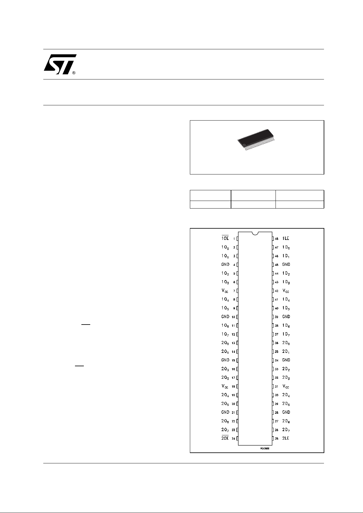
PIN CO NNECTION
TSSOP
DESCRIPTION
The 74LVX16373 is a low voltage CMOS 16 BIT
D-TYPE LATCH with 3 STATE OUTPUTS NON
INVERTING fabricated with sub-micron silicon
gate and double-layer metal wiring C
2
MOS
technology. It is i deal for low power, battery
operated and low noise 3.3V applications.
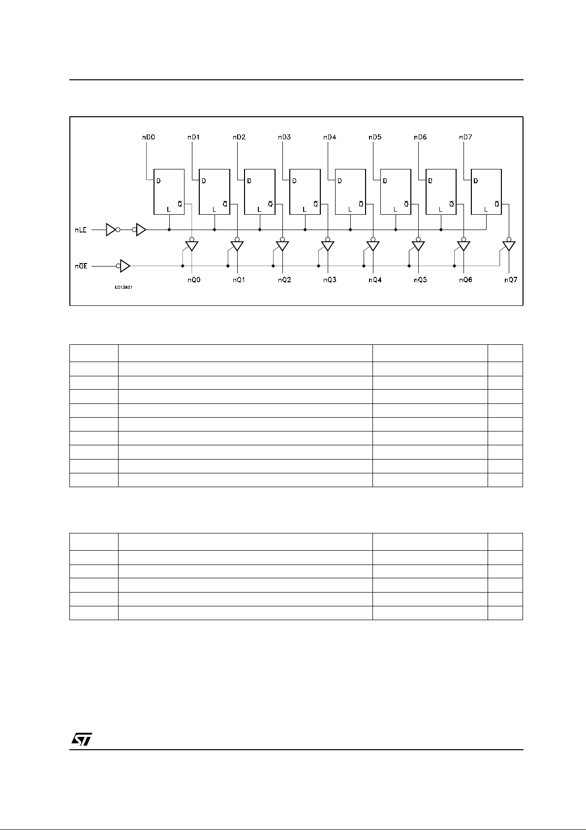
These 16 bit D-TYPE latches are byte controll ed
by two latc h enable inputs (nLE) and two out put
enable inputs(OE
).
While the nLE input is held at a high level, the nQ
outputs will follow the data input precisely.
When the nLE is taken LOW, the nQ outputs will
be latched precisely at the lo gic level of D input
data.
While the (nOE
) input is low, the nQ outputs will be
in a normal logic state (high or low logic level) and
while high leve l the outputs will be in a high impedance state.
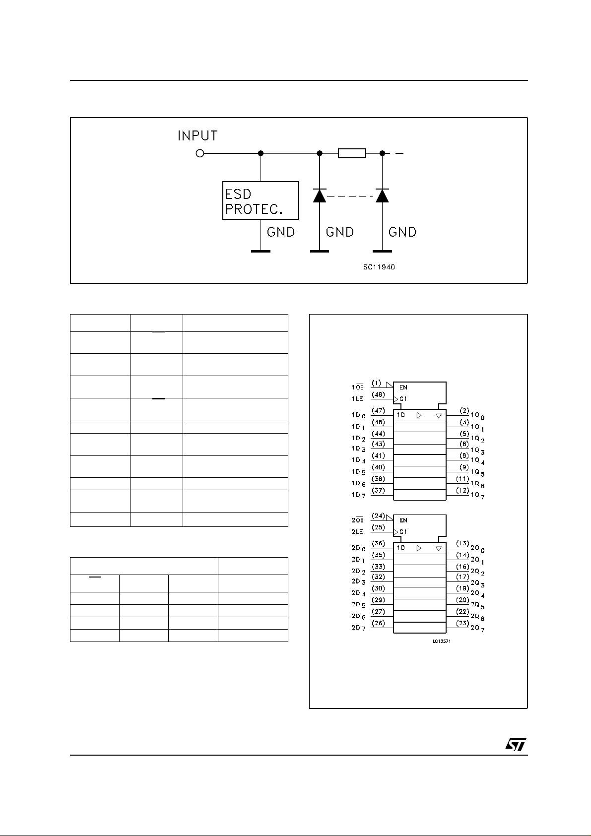
Power down protection is provided on all inputs
and 0 to 7V can be accepted on inputs with no
regard to the suppl y voltage.
This device can be used to interface 5V to 3V. It
combines high speed performance with the true
CMOS low power consumption.
All inputs and outputs are equipped with protection circuits against static discharge, giving them
2KV ESD immunity and transient excess vo ltage.
1/10February 2003
74LVX16373
INPUT EQUIVALENT CIRCUIT
PIN DESCRIPTION
PIN No SYMBOL NAME AND FUNCTION
1 1OE
2, 3, 5, 6, 8, 9,
11, 12
13,14, 16, 17,
19, 20, 22, 23
24 2OE
25 2LE Latch Enable Input
36,35, 33, 32,
30, 29, 27, 26
47,46, 44, 43,
41, 40, 38, 37
48 1LE Latch Enable Input
4, 10, 15, 21,
28, 34, 39, 45
7, 18, 31, 42 V
1Q0 to 1Q7 3-State Outputs
2Q0 to 2Q7 3-State Outputs
2D0 to 2D7 Data Inputs
1D0 to 1D7 Data Inputs
GND Ground (0V)
CC
3 State Output Enable
Input (Active LOW)
3 State Output Enable
Input (Active LOW)
Positive Supply Voltage
TRUTH TABLE
INPUTS OUTPUT
OE
HXX Z
L L X NO CHANGE *
LHL L
LHH H
X : Don‘t Care
Z : High Impedance
* : Qoutputs are latched at thetime when the LE input istaken low
logiclevel.
LE D Q
IEC LOGIC SYMBOLS
2/10
74LVX16373
LOGIC DIAGRAM
This logic diagram has not to be used to estimate propagation delays
ABSOLUTE MAXIMUM RATINGS
Symbol Parameter Value Unit
V
V
V
I
I
OK
I
or I
I
CC
T
T
Absolute Maximum Ratings are those values beyond which damage to the device may occur. Functional operation under these conditions is
not implied
Supply Voltage
CC
DC Input Voltage
I
DC Output Voltage -0.5 to VCC+ 0.5
O
DC Input Diode Current
IK
DC Output Diode Current
DC Output Current
O
DC VCCor Ground Current
GND
Storage Temperature
stg
Lead Temperature (10 sec)
L
-0.5 to +7.0 V
-0.5 to +7.0 V
V
-20 mA
± 20 mA
± 25 mA
± 50 mA
-65 to +150 °C
300 °C
RECOMMENDED OPERATING CONDITIONS
Symbol Parameter Value Unit
V
V
V
T
dt/dv
1) Truth Table guaranteed: 1.2V to 3.6V
2) V
from0.8V to 2.0V
IN
Supply Voltage (note 1)
CC
Input Voltage
I
Output Voltage 0 to V
O
Operating Temperature
op
Input Rise and Fall Time (note 2) (V
CC
=3V)
2 to 3.6 V
0 to 5.5 V
CC
-55 to 125 °C
0 to 100 ns/V
V
3/10
 Loading...