

SGS Thomson Microelectronics 74LVX125MTR, 74LVX125M, 74LVX125TTR Datasheet
1/9July 2001
■ HIGH SPEED: t
PD
=4.4ns (TYP.) at VCC = 3.3V
■ 5V TOLERANT INPUTS
■ POWER-DOWN PROTECTION ON INPUTS
■ INPUT VOLTAGE LEVEL:
V
IL
= 0.8V, VIH = 2V at VCC =3V
■ LOW POWER DISSIPATION:
I
CC
= 2 µA (MAX.) at TA=25°C
■ LOW NOISE:
V
OLP
= 0.3V (TYP.) at VCC =3.3V
■ SYMMETRICAL OUTPUT IMPEDANCE:
|I
OH
| = IOL = 4 mA (MIN) at VCC =3V
■ BALANCED PROPAGATION DELAYS:
t
PLH
≅ t
PHL
■ OPERATING VOLTAGE RANGE:
V
CC
(OPR) = 2V to 3.6V (1.2V Data Retention)
■ PIN AND FUNCTION COMPATIBLE WITH
74 SERIES 125
■ IMPROVED LATCH-UP IMMUNITY
DESCRIPTION
The 74LVX125 is a low voltage CMOS QUAD
BUS BUFFERs fabricated with sub-micron silic on
gate and double-layer metal wiring C
2
MOS
technology. It is ideal for low power, battery
operated and low noise 3.3V applications.
This device requires the 3-STATE control input G
to be set high to place the output into the high
impedance state.
Power down protection is provided on all inputs
and 0 to 7V can be accepted on inputs with no
regard to the supply voltage. This device can be
used to interface 5V to 3V. It combines high
speed performance with the true CMOS low
power consumption.
All inputs and outputs are equipped with
protection circuits against stat ic discharge, giving
them 2KV ESD immunity and transient excess
voltage.
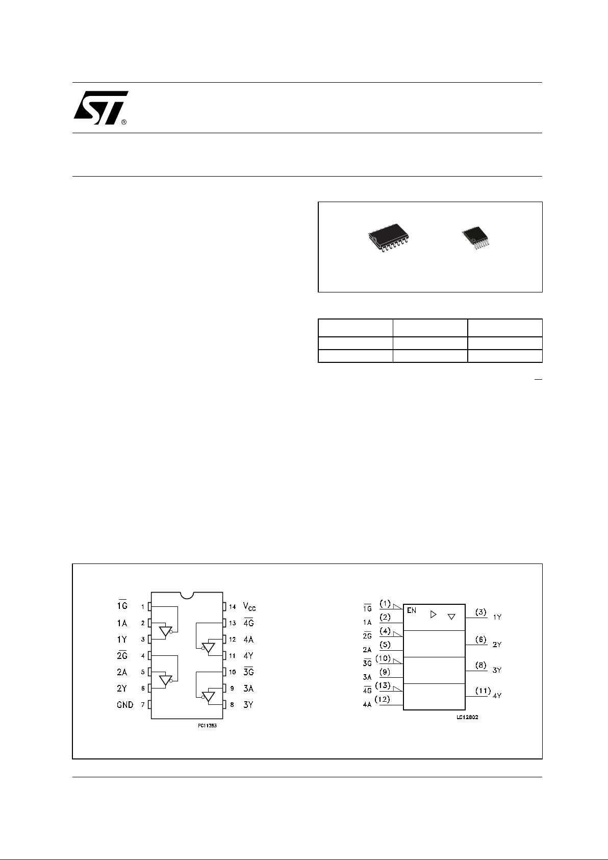
74LVX125
LOW VOLTAGE QUAD BUS BUFFERS (3-STATE)
WITH 5V TOLERANT INPUTS
PIN CONNECTION AND IEC LOGIC SYMBOLS
ORDER CODES
PACKAGE TUBE T & R
SOP 74LVX125M 74LVX125MTR
TSSOP 74LVX125TTR
TSSOPSOP
74LVX125
2/9
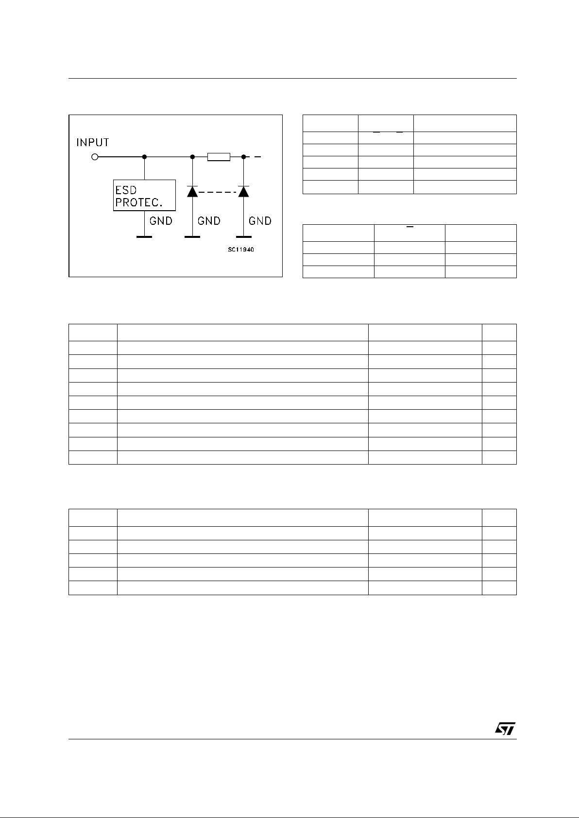
INPUT EQUIVALENT CIRCUIT PIN DESCRIPTION
TRUTH TABLE
X :Don‘t Care
Z : High Impedance
ABSOLUTE MAXIMUM RATINGS
Absolute Maximum Ratings are those values beyond which damage to the device may occur. Functional operation under these conditions is
not implied
RECOMMENDED OPERATING CONDITIONS
1) Truth T abl e guarante ed: 1.2V to 3.6 V
2) V
IN
from 0.8V to 2.0V
PIN No SYMBOL NAME AND FUNCTION
1, 4, 10, 13 1G
to 4G Output Enable Inputs
2, 5, 9, 12 1A to 4A Data Inputs
3, 6, 8, 11 1Y to 4Y Data Outputs
7 GND Ground (0V)
14
V
CC
Positive Supply Voltage
AG
Y
XHZ
LLL
HLH
Symbol Parameter Value Unit
V
CC
Supply Voltage
-0.5 to +7.0 V
V
I
DC Input Voltage
-0.5 to +7.0 V
V
O
DC Output Voltage -0.5 to VCC + 0.5
V
I
IK
DC Input Diode Current
- 20 mA
I
OK
DC Output Diode Current
± 20 mA
I
O
DC Output Current
± 25 mA
I
CC
or I
GND
DC VCC or Ground Current
± 50 mA
T
stg
Storage Temperature
-65 to +150 °C
T
L
Lead Temperature (10 sec)
300 °C
Symbol Parameter Value Unit
V
CC
Supply Voltage (note 1)
2 to 3.6 V
V
I
Input Voltage
0 to 5.5 V
V
O
Output Voltage 0 to V
CC
V
T
op
Operating Temperature
-55 to 125 °C
dt/dv
Input Rise and Fall Time (note 2) (V
CC
= 3V)
0 to 100 ns/V
74LVX125
3/9
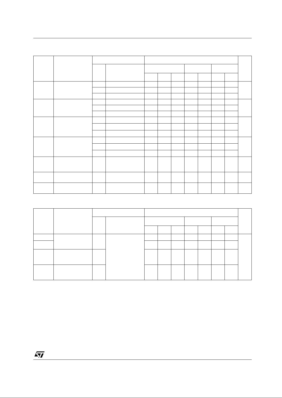
DC SPECIFICATIONS
DYNAMIC SWITCHING CHARACTERISTICS
1) Worst c ase package .
2) Max number of outp ut s defined as (n). Data inputs are driven 0V to 3.3V, (n-1) outputs switching and one output at GND.
3) Max number of data inputs (n) switching. (n-1) switching 0V to 3.3V. Inputs under test switching: 3.3V to threshold (V
ILD
), 0V to threshold
(V
IHD
), f=1MHz.
Symbol Parameter
Test Condition Value
Unit
V
CC
(V)
T
A
= 25°C
-40 to 85°C -55 to 125°C
Min. Typ. Max. Min. Max. Min. Max.
V
IH
High Level Input
Voltage
2.0 1.5 1.5 1.5
V3.0
2.0 2.0 2.0
3.6
2.4 2.4 2.4
V
IL
Low Level Input
Voltage
2.0 0.5 0.5 0.5
V3.0 0.8 0.8 0.8
3.6 0.8 0.8 0.8
V
OH
High Level Output
Voltage
2.0
IO=-50 µA
1.9 2.0 1.9 1.9
V3.0
I
O
=-50 µA
2.9 3.0 2.9 2.9
3.0
I
O
=-4 mA
2.58 2.48 2.4
V
OL
Low Level Output
Voltage
2.0
I
O
=50 µA
0.0 0.1 0.1 0.1
V3.0
I
O
=50 µA
0.0 0.1 0.1 0.1
3.0
I
O
=4 mA
0.36 0.44 0.55
I
OZ
High Impedance
Output Leakage
Current
3.6
V
I
= VIH or V
IL
VO = VCC or GND
±0.25 ± 2.5 ± 5 µA
I
I
Input Leakage
Current
3.6
V
I
= 5.5V or GND
± 0.1 ± 1 ± 1 µA
I
CC
Quiescent Supply
Current
3.6
V
I
= VCC or GND
22020µA
Symbol Parameter
Test Condition Value
Unit
V
CC
(V)
T
A
= 25°C
-40 to 85°C -55 to 125°C
Min. Typ. Max. Min. Max. Min. Max.
V
OLP
Dynamic Low
Voltage Quiet
Output (note 1, 2)
3.3
C
L
= 50 pF
0.3 0.5
V
V
OLV
-0.5 -0.3
V
IHD
Dynamic High
Voltage Input
(note 1, 3)
3.3 2.0
V
ILD
Dynamic Low
Voltage Input
(note 1, 3)
3.3 0.8
 Loading...