

1/8July 2001
■ HIGH SPEED :
t
PD
= 4.8ns (TYP.) at V
CC
= 3.3V
■ 5V TOLERANT INPUTS
■ INPUT VOLTAGE LEVEL :
V
IL
=0.8V , VIH=2V at VCC=3V
■ LOW POWER DISSIPATION:
I
CC
= 2 µA (MAX.) at TA=25°C
■ LOW NOISE:
V
OLP
= 0.3V (TYP.) at VCC = 3.3V
■ OPERATING VOL TAGE RANGE:
V
CC
(OPR) = 2V to 3.6V (1.2V Data Retention)
■ PIN AND FUNCTION COMPATIBLE WITH
74 SERIES 05
■ IMPROVED LATCH-UP IMMUNITY
■ POWER DOWN PROTECTION ON INPUTS
DESCRIPTION
The 74LVX05 is a low voltage CMOS OPEN
DRAIN HEX INVERTER fabricated with
sub-micron silicon gate and double-layer metal
wiring C
2
MOS technology. It is ideal for low
power, battery operated and low noise 3.3V
applications.
The internal circuit is composed of 3 stages
including buffer ou tput, which provides high noise
immunity and stable output.
Power down protection is provided on all inputs
and 0 to 7V can be accepted on inputs with no
regard to the supply voltage.
This device can be used to interface 5V to 3V
system. It combines high speed performance with
the true CMOS low power consumption.
All inputs and outputs are equipped with
protection circuits against stat ic discharge, giving
them 2KV ESD immunity and transient excess
voltage.
74LVX05
LOW VOLTAGE CMOS HEX INVERTER (OPEN DRAIN)
WITH 5V TOLERANT INPUTS
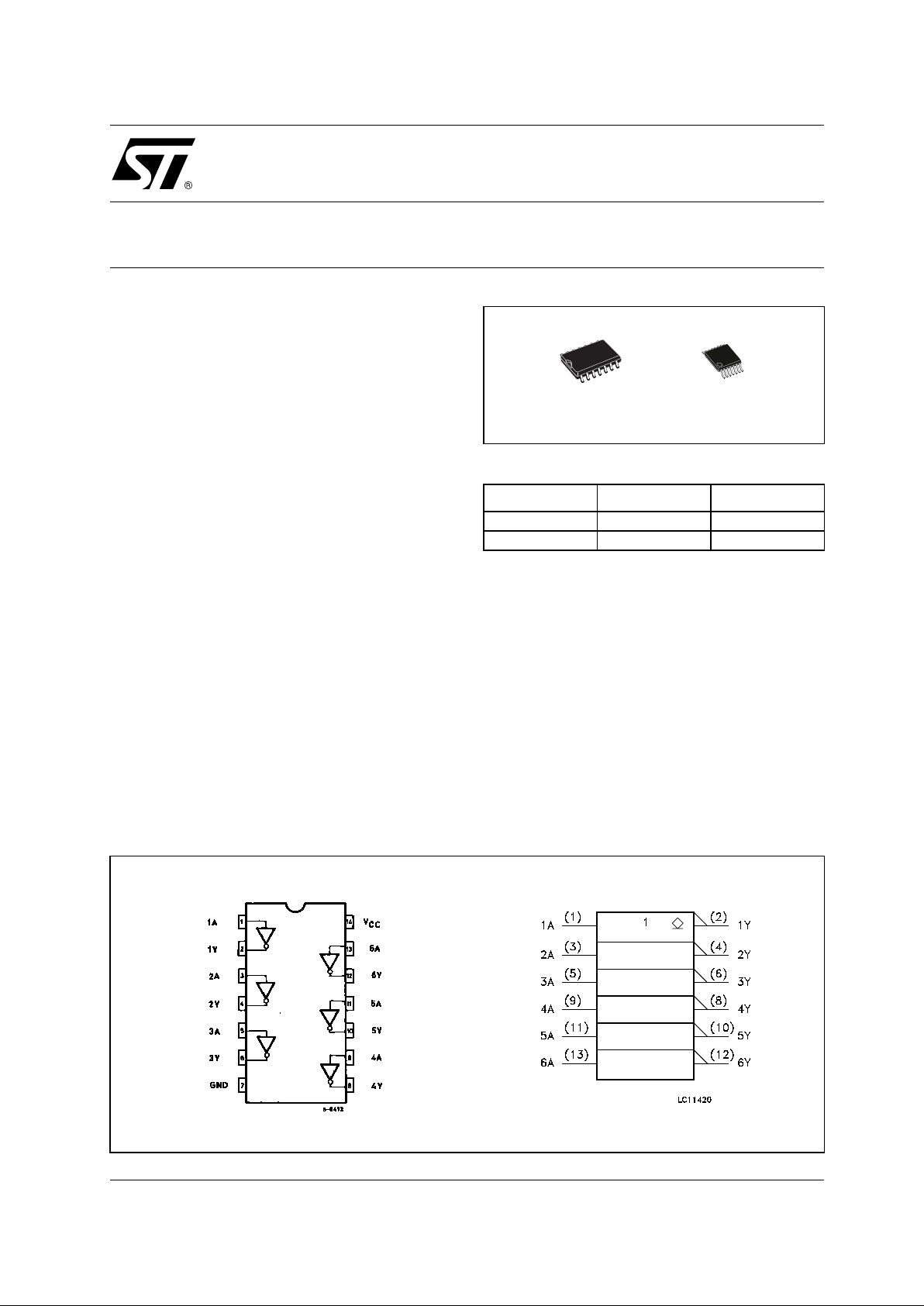
PIN CONNECTION AND IEC LOGIC SYMBOLS
ORDER CODES
PACKAGE TUBE T & R
SOP 74LVX05M 74LVX05MTR
TSSOP 74LVX05TTR
TSSOPSOP
74LVX05
2/8
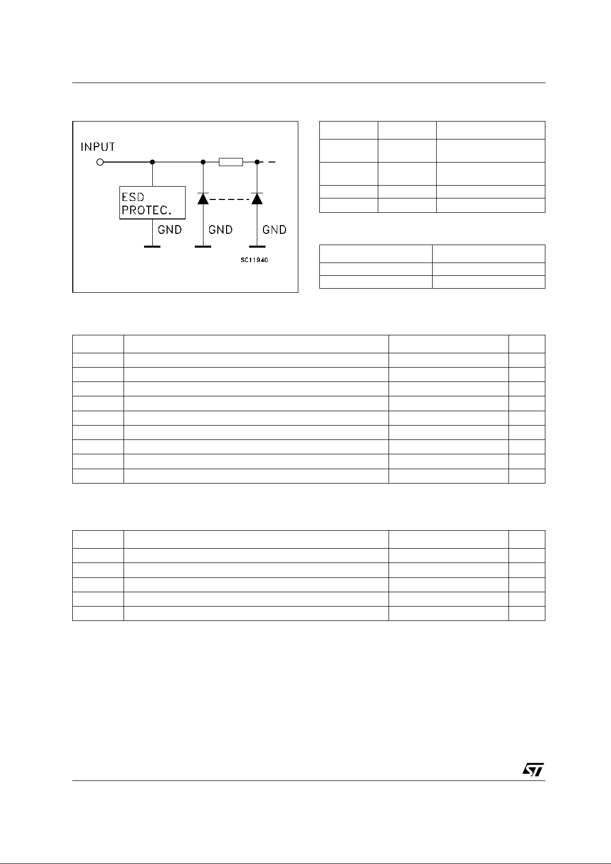
INPUT EQUIVALENT CIRCUIT PIN DESCRIPTION
TRUTH TABLE
Z: High Impedance
ABSOLUTE MAXIMUM RATINGS
Absolute Maximum Ratings are those values beyond which damage to the device may occur. Functional operation under these conditions is
not implied.
RECOMMENDED OPERATING CONDITIONS
1) Truth T abl e guarante ed: 1.2V to 3.6 V
2) V
IN
from 0.8V to 2.0V
PIN No SYMBOL NAME AND FUNCTION
1, 3, 5, 9, 1 1,
13
1A to 6A Data Inputs
2, 4, 6, 8, 10,
12
1Y to 6Y Data Outputs
7 GND Ground (0V)
14
V
CC
Positive Supply Voltage
AY
LZ
HL
Symbol Parameter Value Unit
V
CC
Supply Voltage
-0.5 to +7.0 V
V
I
DC Input Voltage
-0.5 to +7.0 V
V
O
DC Output Voltage -0.5 to VCC + 0.5
V
I
IK
DC Input Diode Current
- 20 mA
I
OK
DC Output Diode Current
± 20 mA
I
O
DC Output Current
± 25 mA
I
CC
or I
GND
DC VCC or Ground Current
± 50 mA
T
stg
Storage Temperature
-65 to +150 °C
T
L
Lead Temperature (10 sec)
300 °C
Symbol Parameter Value Unit
V
CC
Supply Voltage (note 1)
2 to 3.6 V
V
I
Input Voltage
0 to 5.5 V
V
O
Output Voltage 0 to V
CC
V
T
op
Operating Temperature
-55 to 125 °C
dt/dv
Input Rise and Fall Time (note 2) (V
CC
= 3.3V)
0 to 100 ns/V
74LVX05
3/8
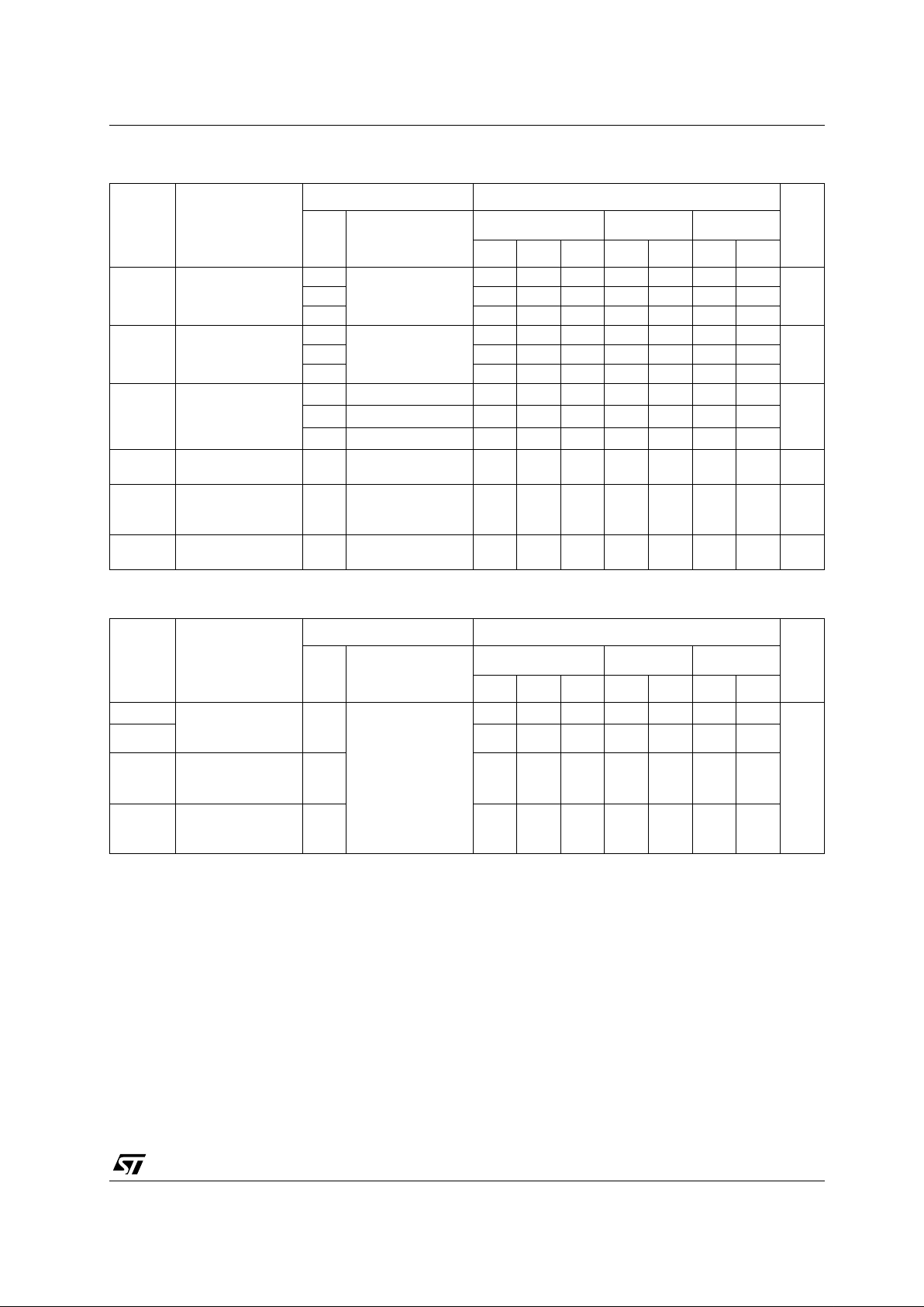
DC SPECIFICATIONS
DYNAMIC SWITCHING CHARACTERISTICS
1) Worst c ase package .
2) Max number of outp ut s defined as (n). Data inputs are driven 0V to 3.3V, (n-1) outputs switching and one output at GND.
3) Max number of data inputs (n) switching. (n-1) switching 0V to 3.3V. Inputs under test switching: 3.3V to threshold (V
ILD
), 0V to threshold
(V
IHD
), f=1MHz.
Symbol Parameter
Test Condition Value
Unit
V
CC
(V)
T
A
= 25°C
-40 to 85°C -55 to 125°C
Min. Typ. Max. Min. Max. Min. Max.
V
IH
High Level Input
Voltage
2.0 1.5 1.5 1.5
V3.0 2.0 2.0 2.0
3.6 2.4 2.4 2.4
V
IL
Low Level Input
Voltage
2.0 0.5 0.5 0.5
V3.0 0.8 0.8 0.8
3.6 0.8 0.8 0.8
V
OL
Low Level Output
Voltage
2.0
IO=50 µA
0.0 0.1 0.1 0.1
V3.0
I
O
=50 µA
0.0 0.1 0.1 0.1
3.0
I
O
=4 mA
0.36 0.44 0.55
I
I
Input Leakage
Current
3.6
V
I
= 5V or GND
± 0.1 ± 1 ± 1 µA
I
OZ
High Impedance
Output Leakage
Current
3.6
V
I
= VIH or V
IL
VO = VCC or GND
±0.25 ± 2.5 ± 5 µA
I
CC
Quiescent Supply
Current
3.6
V
I
= VCC or GND
22020µA
Symbol Parameter
Test Condition Value
Unit
V
CC
(V)
T
A
= 25°C
-40 to 85°C -55 to 125°C
Min. Typ. Max. Min. Max. Min. Max.
V
OLP
Dynamic Low
Voltage Quiet
Output (note 1, 2)
3.3
C
L
= 50 pF
0.3 0.5
V
V
OLV
-0.5 -0.3
V
IHD
Dynamic High
Voltage Input (note
1, 3)
3.3 2
V
ILD
Dynamic Low
Voltage Input (note
1, 3)
3.3 0.8
 Loading...