

74LVX04
LOW VOLTAGE CMOS HEX INVERTER
WITH 5V TOLERANT INPUTS
■ HIGH SPEED :
t
= 4.1ns (TYP.) at V
PD
■ 5V TOLERANT INPUTS
■ INPUT VOLTAGE LEVEL :
=0.8V , VIH=2V at VCC=3V
V
IL
■ LOW POWER DISSIPATION:
I
= 2 µA (MAX.) at TA=25°C
CC
■ LOW NOISE:
V
= 0.3V (TYP.) at VCC = 3.3V
OLP
■ SYMMETRICAL OUTPUT IMPEDANCE:
|I
| = IOL = 4mA (MIN)
OH
■ BALANCED PROPAGATION DELAYS:
t
≅ t
PLH
■ OPERATING VOL TAGE RANGE:
V
CC
■ PIN AND FUNCTION COMPATIBLE WITH
PHL
(OPR) = 2V to 3.6V (1.2V Data Retention)
CC
= 3.3V
74 SERIES 04
■ IMPROVED LATCH-UP IMMUNITY
■ POWER DOWN PROTECTION ON INPUTS
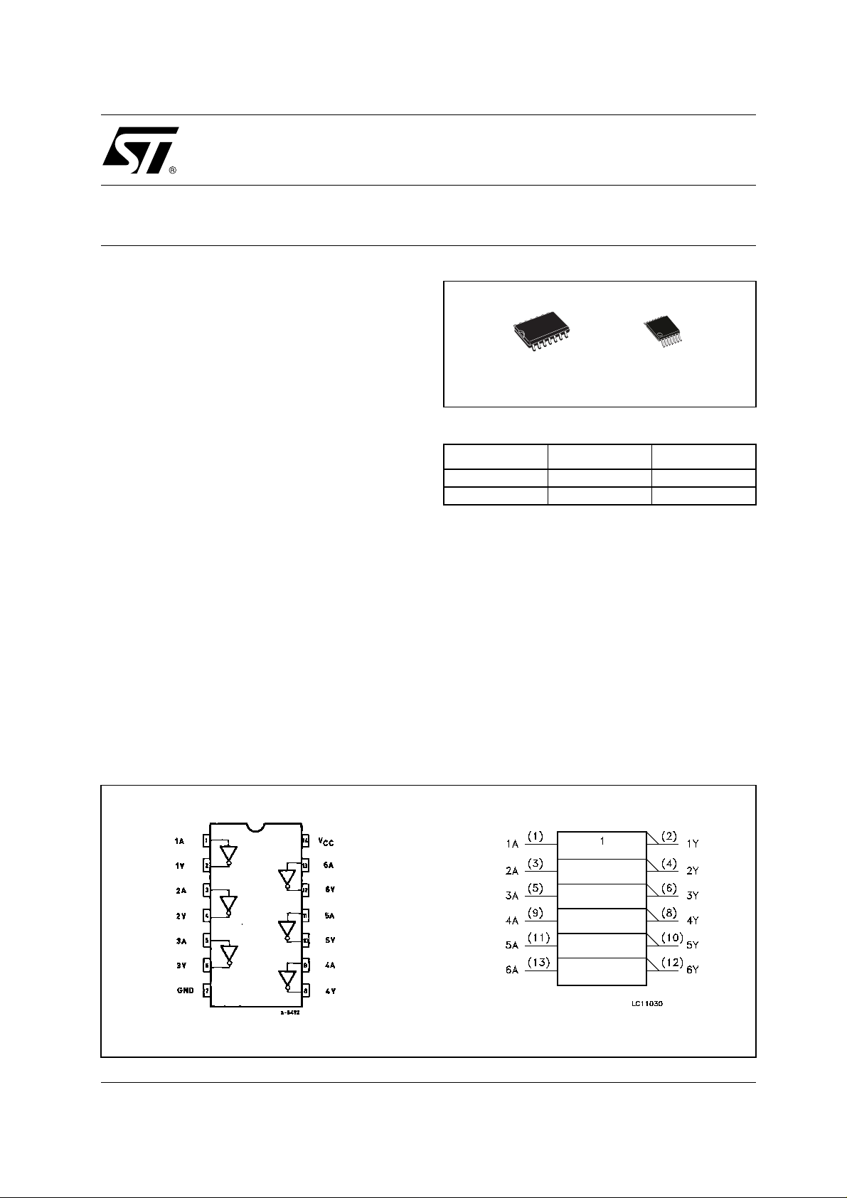
DESCRIPTION
The 74LVX04 is a low voltage CMOS HEX
INVERTER fabricated with sub-micron silicon
gate and double-layer metal wiring C
2
MOS
technology. It is ideal for low power, battery
operated and low noise 3.3V applications.
TSSOPSOP
ORDER CODES
PACKAGE TUBE T & R
SOP 74LVX04M 74LVX04MTR
TSSOP 74LVX04TTR
The internal circuit is composed of 3 stages
including buffer ou tput, which provides high noise
immunity and stable output.
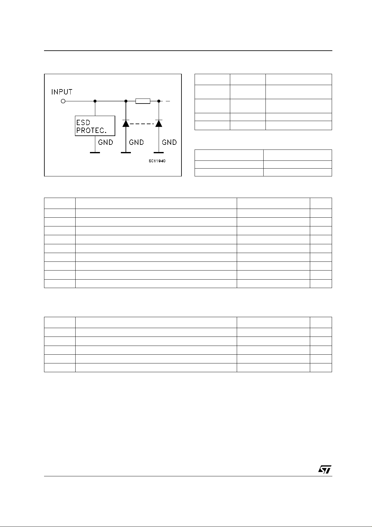
Power down protection is provided on all inputs
and 0 to 7V can be accepted on inputs with no
regard to the supply voltage.
This device can be used to interface 5V to 3V
system. It combines high speed performance with
the true CMOS low power consumption.
All inputs and outputs are equipped with
protection circuits against stat ic discharge, giving
them 2KV ESD immunity and transient excess
voltage.
PIN CONNECTION AND IEC LOGIC SYMBOLS
1/8July 2001
74LVX04
INPUT EQUIVALENT CIRCUIT PIN DESCRIPTION
PIN No SYMBOL NAME AND FUNCTION
1, 3, 5, 9, 1 1,
13
2, 4, 6, 8, 10,
12
7 GND Ground (0V)
14
TRUTH TABLE
ABSOLUTE MAXIMUM RATINGS
Symbol Parameter Value Unit
V
V
V
I
I
OK
I
I
or I
CC
T
T
Absolute Maximum Ratings are those values beyond which damage to the device may occur. Functional operation under these conditions is
not implied.
Supply Voltage
CC
DC Input Voltage
I
DC Output Voltage -0.5 to VCC + 0.5
O
DC Input Diode Current
IK
DC Output Diode Current
DC Output Current
O
DC VCC or Ground Current
GND
Storage Temperature
stg
Lead Temperature (10 sec)
L
1A to 6A Data Inputs
1Y to 6Y Data Outputs
V
CC
Positive Supply Voltage
AY
LH
HL
-0.5 to +7.0 V
-0.5 to +7.0 V
V
- 20 mA
± 20 mA
± 25 mA
± 50 mA
-65 to +150 °C
300 °C
RECOMMENDED OPERATING CONDITIONS
Symbol Parameter Value Unit
V
V
V
T
dt/dv
1) Truth T abl e guarante ed: 1.2V to 3.6 V
2) V
from 0.8V to 2.0V
IN
2/8
Supply Voltage (note 1)
CC
Input Voltage
I
Output Voltage 0 to V
O
Operating Temperature
op
Input Rise and Fall Time (note 2) (V
= 3.3V)
CC
2 to 3.6 V
0 to 5.5 V
CC
-55 to 125 °C
0 to 100 ns/V
V
DC SPECIFICATIONS
Symbol Parameter
V
V
V
V
I
High Level Input
IH
Voltage
Low Level Input
IL
Voltage
High Level Output
OH
Voltage
Low Level Output
OL
Voltage
I
Input Leakage
I
Current
Quiescent Supply
CC
Current
Test Condition Value
V
(V)
CC
= 25°C
A
Min. Typ. Max. Min. Max. Min. Max.
-40 to 85°C -55 to 125°C
T
2.0 1.5 1.5 1.5
3.6 2.4 2.4 2.4
2.0 0.5 0.5 0.5
3.6 0.8 0.8 0.8
2.0
3.0
2.0
3.0
3.6
3.6
IO=-50 µA
I
=-50 µA
O
I
=-4 mA
O
=50 µA
I
O
I
=50 µA
O
I
=4 mA
O
= 5V or GND
V
I
= VCC or GND
V
I
1.9 2.0 1.9 1.9
2.9 3.0 2.9 2.9
2.58 2.48 2.4
0.0 0.1 0.1 0.1
0.0 0.1 0.1 0.1
0.36 0.44 0.55
± 0.1 ± 1 ± 1 µA
22020µA
74LVX04
Unit
V3.0 2.0 2.0 2.0
V3.0 0.8 0.8 0.8
V3.0
V3.0
DYNAMIC SWITCHING CHARACTERISTICS
Test Condition Value
T
Symbol Parameter
V
CC
(V)
V
V
V
Dynamic Low
OLP
Voltage Quiet
OLV
Output (note 1, 2)
Dynamic High
IHD
Voltage Input (note
3.3
3.3 2
= 50 pF
C
L
1, 3)
V
Dynamic Low
ILD
Voltage Input (note
3.3 0.8
1, 3)
1) Worst c ase package .
2) Max number of outp ut s defined as (n). Data inputs are driven 0V to 3.3V, (n-1) outputs switching and one output at GND.
3) Max number of data inputs (n) switching. (n-1) switching 0V to 3.3V. Inputs under test switching: 3.3V to threshold (V
(V
), f=1MHz.
IHD
= 25°C
A
-40 to 85°C -55 to 125°C
Min. Typ. Max. Min. Max. Min. Max.
0.3 0.5
-0.5 -0.3
ILD
Unit
V
), 0V to threshold
3/8
74LVX04
AC ELECTRICAL CHARACTERISTICS (Input tr = tf = 3ns)
Test Condition Value
T
Symbol Parameter
t
PLH tPHL
Propagation Delay
Time
3.3
3.3
t
OSLH
t
OSHL
1) Skew is defined as the absolute value of the difference between the actual propagation delay for any two outputs of the same device switching in the same direction, either HI GH or LOW
2) Param eter guaran teed by design
(*) Vol tage range is 3.3V ±
Output To Output
Skew Time (note1,
2)
0.3V
3.3
C
V
CC
(V)
L
(pF)
2.7 15 5.4 10.1 1.0 12.5 1.0 14.5
2.7 50 7.9 13.6 1.0 16.0 1.0 18.0
(*)
15 4.1 6.2 1.0 7.5 1.0 8.5
(*)
50 6.6 9.7 1.0 11.0 1.0 12.0
2.7 50 0.5 1.0 1.5 1.5
(*)
50
= 25°C
A
Min. Typ. Max. Min. Max. Min. Max.
0.5 1.0 1.5 1.5
CAPACITIVE CHARACTERISTICS
Test Condition Value
T
Symbol Parameter
V
CC
(V)
C
C
Input Capacitance
IN
Power Dissipation
PD
Capacitance
3.3 4101010pF
3.3 18 pF
(note 1)
1) CPD is defined as the value of the IC’s internal equivalent capacitance which is calculated from the operating current consumption without
load. (Refer to Test Circuit). Average operating current can be obtained by the following equation. I
= 25°C
A
Min. Typ. Max. Min. Max. Min. Max.
-40 to 85°C -55 to 125°C
-40 to 85°C -55 to 125°C
= CPD x VCC x fIN + ICC/6 (per gate)
CC(opr)
Unit
ns
ns
Unit
4/8
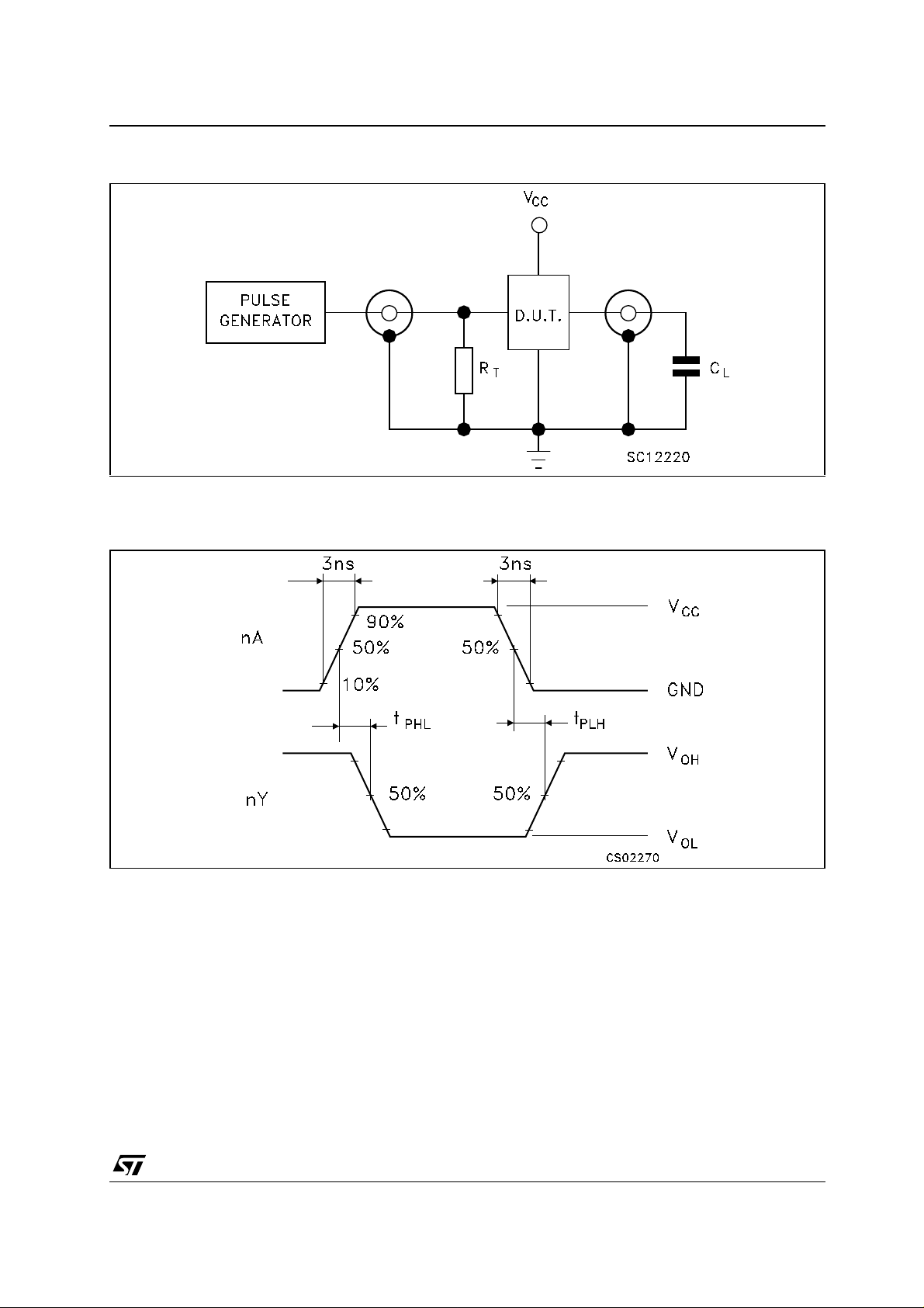
TEST CIRCUIT
CL =15/50pF or equivalent (i ncludes jig and probe cap acitance)
= Z
R
of pulse generator (typically 50Ω)
T
OUT
WAVEFORM: PROPAGATION DELAYS (f=1MHz; 50% duty cycle)
74LVX04
5/8
74LVX04
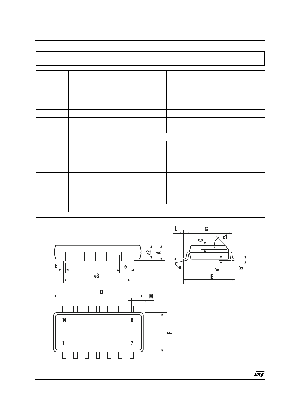
SO-14 MECHANICAL DATA
DIM.
A 1.75 0.068
a1 0.1 0.2 0.003 0.007
a2 1.65 0.064
b 0.35 0.46 0.013 0.018
b1 0.19 0.25 0.007 0.010
C 0.5 0.019
c1 45° (typ.)
D 8.55 8.75 0.336 0.344
E 5.8 6.2 0.228 0.244
e 1.27 0.050
e3 7.62 0.300
F 3.8 4.0 0.149 0.157
G 4.6 5.3 0.181 0.208
L 0.5 1.27 0.019 0.050
M 0.68 0.026
S8° (max.)
MIN. TYP MAX. MIN. TYP. M AX.
mm. inch
6/8
PO13G
74LVX04
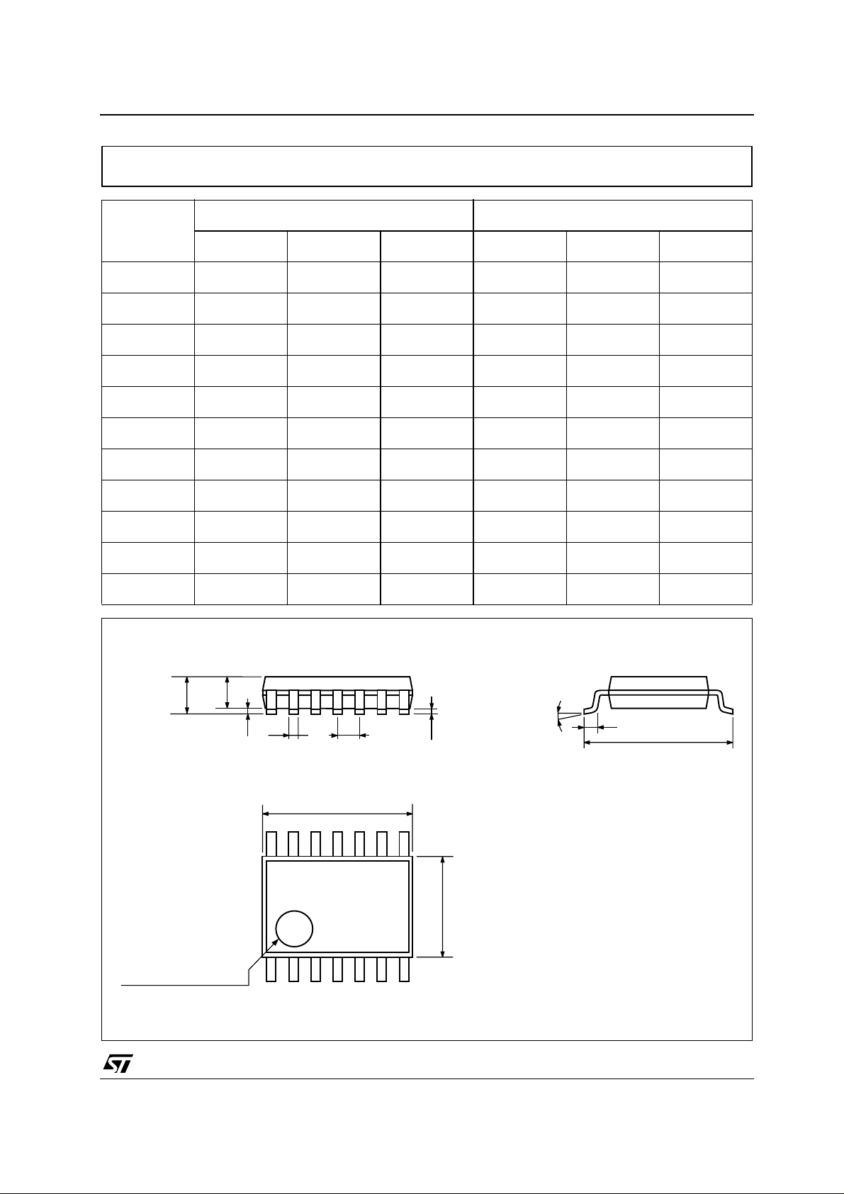
TSSOP14 MECHANICAL DATA
mm. inch
DIM.
MIN. TYP MAX. MIN. TYP. M AX.
A 1.2 0.047
A1 0.05 0.15 0.002 0.004 0.006
A2 0.8 1 1.05 0.031 0.039 0.041
b 0.19 0.30 0.007 0.012
c 0.09 0.20 0.004 0.0089
D 4.9 5 5.1 0.193 0.197 0.201
E 6.2 6.4 6.6 0.244 0.252 0.260
E1 4.3 4.4 4.48 0.169 0.173 0.176
e 0.65 BSC 0.0256 BSC
K0° 8°0° 8°
L 0.45 0.60 0.75 0.018 0.024 0.030
A2
A
A1
b
e
c
K
L
E
D
E1
PIN 1 IDENTIFICATION
1
0080337D
7/8

74LVX04
Information furnished is bel ieved to be accurate and reliable. However, STMicroe lectronics assumes no responsibility for the
consequences of use of such information nor for any infringement of patents or other rights of third parties which may result from
its use. No li cense is granted by implication or otherwise unde r any patent or patent rights of STMicroelectronics. Specifications
mentioned in this publication ar e subject to change without notice. This publication supersedes and replaces all information
previously supplied. S TMicroelectronics products are not authorized for use as critica l components in life suppo rt devices or
systems without express written approval of STMicroelectronics.
Australi a - Brazil - Chi na - Finlan d - F rance - Germany - Hong Kong - India - Ital y - Japan - Ma l aysia - Malta - Morocco
© The ST logo is a registered trademark of STMicroelectronics
© 2001 STM icroelectronics - Pr inted in Ital y - All Rights Reserved
STMicr o el ectronics GROUP OF COMPANIES
Singapo re - Spain - Sweden - Swit zerland - Un i ted Kingdom
© http://www.st.com
8/8
 Loading...