

SGS Thomson Microelectronics 74LVQ573 Datasheet
74LVQ573
OCTAL D-TYPE LATCH
WITH 3 STATE OUTPUTSNON INVERTING
■ HIGHSPEED:t
■ COMPATIBLEWITHTTLOUTPUTS
■ LOW POWERDISSIPATION:
I
=4µA (MAX.)at TA=25oC
CC
■
LOWNOISE:
=0.5 V (TYP.)at VCC=3.3V
V
OLP
■ 75Ω TRANSMISSIONLINEDRIVING
=5 ns(TYP.)atVCC=3.3V
PD
CAPABILITY
■
SYMMETRICALOUTPUTIMPEDANCE:
|=IOL=24mA(MIN)
|I
OH
■
PCIBUSLEVELSGUARANTEEDAT 24mA
■ BALANCEDPROPAGAT IONDELAYS:
≅ t
t
PLH
PHL
■ OPERATINGVOLTAGERANGE:
V
(OPR)= 2Vto3.6V(1.2VDataRetention)
CC
■
PINANDFUNCTION COMPATIBLEWITH
74SERIES573
■ IMPROVEDLATCH-UP IMMUNITY
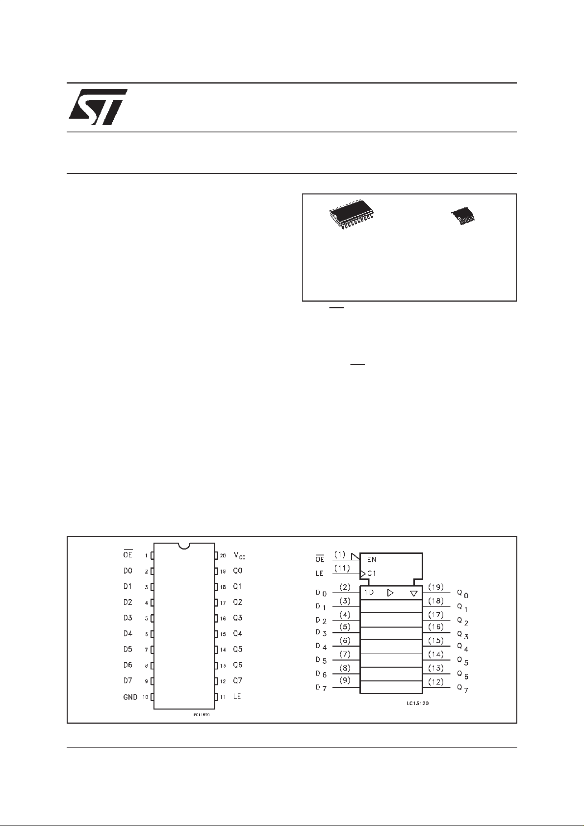
DESCRIPTION
The LVQ573 is a low voltage CMOS OCTAL
D-TYPE LATCH with 3 STATE OUTPUT NON
INVERTING fabricated with sub-micron silicon
gate and double-layer metal wiring C
2
MOS
technology. It is ideal for low power and low
noise 3.3Vapplications.
These 8 bit D-Type flip-flops are controlled by a
latch enable input (LE) and an output enable
M
(Micro Package)
(TSSOPPackage)
T
ORDERCODES :
74LVQ573M 74LVQ573T
input (OE).
While the LE input is held at a high level, the Q
outputswill follow the data input precisely.
When the LE is taken low, the Q outputs will be
latchedpreciselyat thelogic level of D input data.
While the (OE) input is low, the 8 outputs will be
in a normal logic state (high or low logic level)
and while high level the outputs will be in a high
impedancestate.
It has better speed performance at 3.3V than 5V
LSTTL family combined with the true CMOS low
powerconsumption.
All inputs and outputs are equipped with
protection circuits against static discharge, giving
them 2KV ESD immunity and transient excess
voltage.
PIN CONNECTION AND IEC LOGIC SYMBOLS
February 1999
1/10
74LVQ573
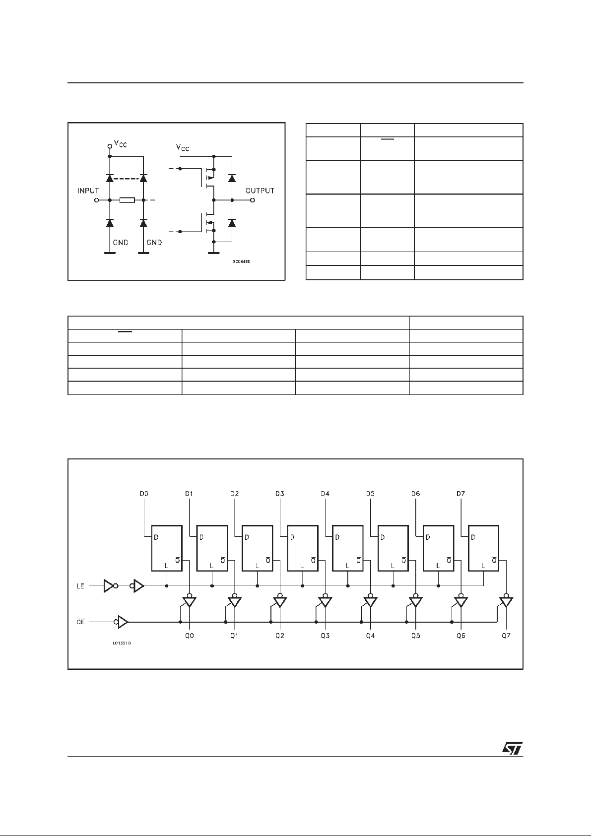
INPUT AND OUTPUTEQUIVALENT CIRCUIT PIN DESCRIPTION
PI N No SYMB OL NAME AND F U NCTION
1 OE 3 State Output Enable
2, 3, 4,
5, 6, 7,
8, 9
12, 13, 14,
15, 16, 17,
18, 19
11 LE Latch Enable
10 GND Ground (0V)
20 V
TRUTH TABLE
INPUTS OUTPUTS
OE LE D Q
HXXZ
L L X NO CHANGE *
LHLL
LHHH
X:Don’tcare
Z:Highimpedance
*Qoutputs arelatched atthetime whentheLEinput Istaken lowlogiclevel.
D0 to D7 Data Inputs
Q0 to Q7 3 State Latch Outputs
CC
Input (Active LOW)
Input
Positive Supply Voltage
LOGICDIAGRAM
2/10
74LVQ573
ABSOLUTE MAXIMUM RATINGS
Symb o l Paramet er Val u e Uni t
V
V
V
I
I
OK
I
or I
I
CC
T
T
AbsoluteMaximumRatingsarethosevaluesbeyond whichdamagetothedevice mayoccur. Functionaloperationunderthesecondition isnotimplied.
RECOMMENDED OPERATINGCONDITIONS
Symb o l Paramet er Value Un it
V
V
V
T
dt/dv Input Rise and Fall Time (V
1) TruthTable guaranteed: 1.2Vto 3.6V
2)V
from0.8V to 2V
IN
Supply Voltage -0.5 to +7 V
CC
DC Input Voltage -0.5 to VCC+ 0.5 V
I
DC Output Voltage -0.5 to VCC+ 0.5 V
O
DC Input Diode Current
IK
20 mA
±
DC Output Diode Current ± 20 mA
DC Output Current ± 50 mA
O
DC VCCor Ground Current ± 400 mA
GND
Storage Temperature -65 to +150
stg
Lead Temperature (10 sec) 300
L
Supply Voltage (note 1) 2 to 3.6 V
CC
Input Voltage 0 to V
I
Output Voltage 0 to V
O
Operating Temperature: -40 to +85
op
= 3V) (note 2) 0 to 10 ns/V
CC
CC
CC
o
C
o
C
V
V
o
C
3/10
 Loading...