

SGS Thomson Microelectronics 74LVQ374 Datasheet
74LCX374
OCTAL D-TYPE FLIP FLOP NON INVERTING (3-STATE)
WITH 5V TOLERANT INPUTS AND OUTPUTS
■ 5VTOLERANTINPUTSAND OUTPUTS
■
HIGHSPEED:
f
=150MHz(MIN.) atVCC=3V
MAX
■
POWER-DOWNPROTECTIONONINPUTS
ANDOUTPUTS
■ SYMMETRICALOUTPUTIMPEDANCE:
|=IOL=24mA(MIN)
|I
OH
■ PCIBUSLEVELSGUARANTEEDAT24mA
■ BALANCEDPROPAGATIONDELAYS:
t
≅ t
PLH
PHL
■ OPERATINGVOLTAGERAN GE:
(OPR)= 2.0Vto3.6V (1.5VDataRetention)
V
CC
■ PINANDFUNCTIONCOMPATIBLEWITH
74SERIES374
■ LATCH-UPPERFORMANCEEXCEEDS500mA
■ ESDPERFORMANCE:
HBM>2000V;MM>200V
DESCRIPTION
The LCX374 is a low voltage CMOS OCTAL
D-TYPE FLIP FLOP with 3 STATE OUTPUT
NON INVERTING fabricated with sub-micron
silicon gate and double-layermetal wiring C
2
MOS
technology. It is ideal for low power and high
speed applications; it can be interfaced to 5V
signal environment for both inputs and outputs.
These 8 bit D-Type flip-flops are controlled by a
clockinput (CK)and anoutput enable input (OE).
On the positive transition of the clock, the Q
(Micro Package)
outputs will be set to the logic state that were
setupat the D inputs.
While the (OE) input is low, the 8 outputs will be
in a normal state (high or low logic level) and
while high level the outputs will be in a high
impedancestate.
The output control does not affect the internal
operation of flip flops; that is, the old data can be
retained or the new data can be entered even
whiletheoutputsare off.
It has same speed performance at 3.3V than 5V,
AC/ACT family, combined with a lower power
consumption. It has better speed performance at
3.3V than 5V LSTTL family combined with the
trueCMOS low powerconsumption.
All inputs and outputs are equipped with
protection circuits against static discharge, giving
them 2KV ESD immunity and transient excess
voltage.
M
T
(TSSOPPackage)
ORDERCODES :
74LCX374M 74LCX374T
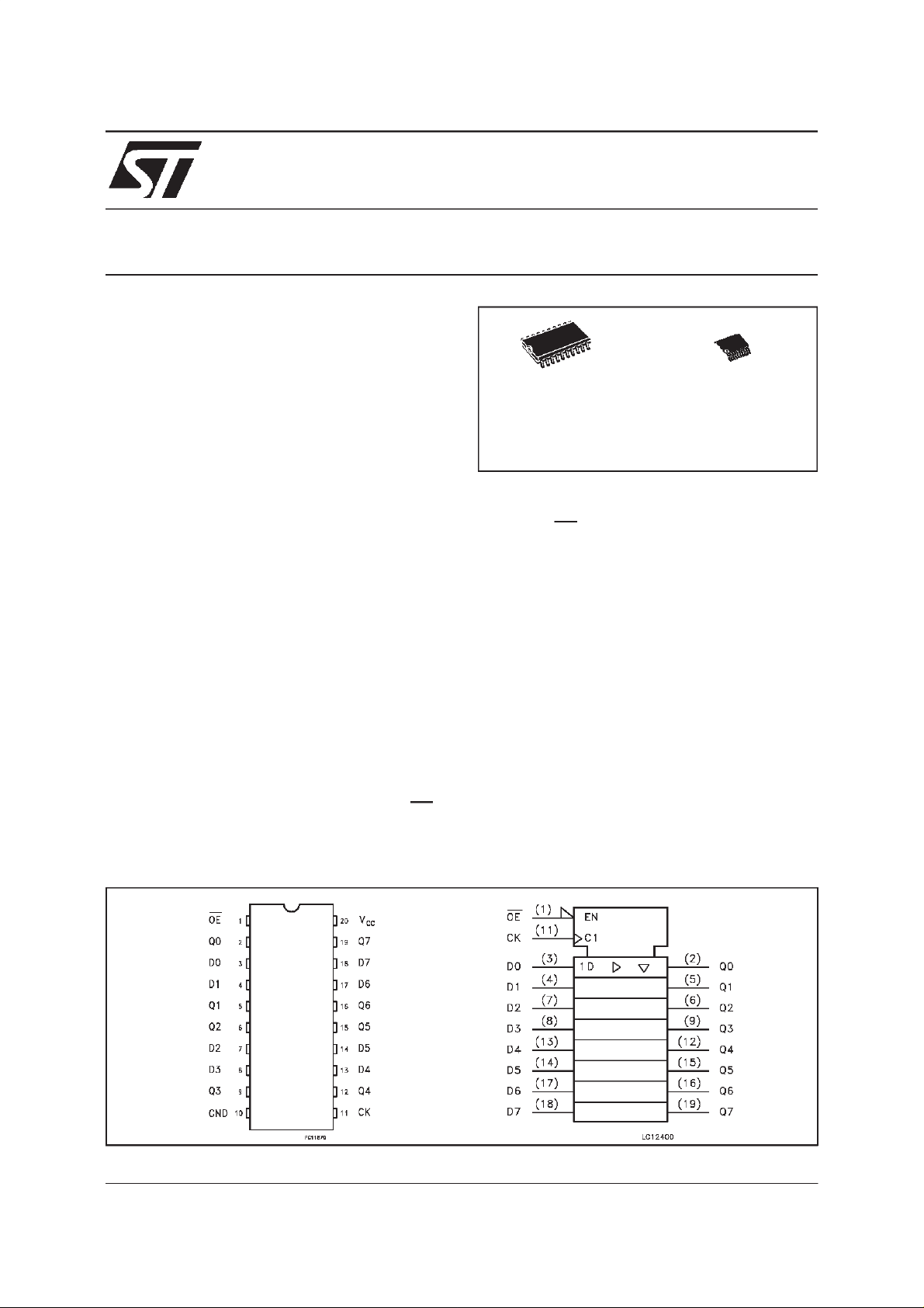
PIN CONNECTION AND IEC LOGIC SYMBOLS
February 1999
1/10
74LCX374
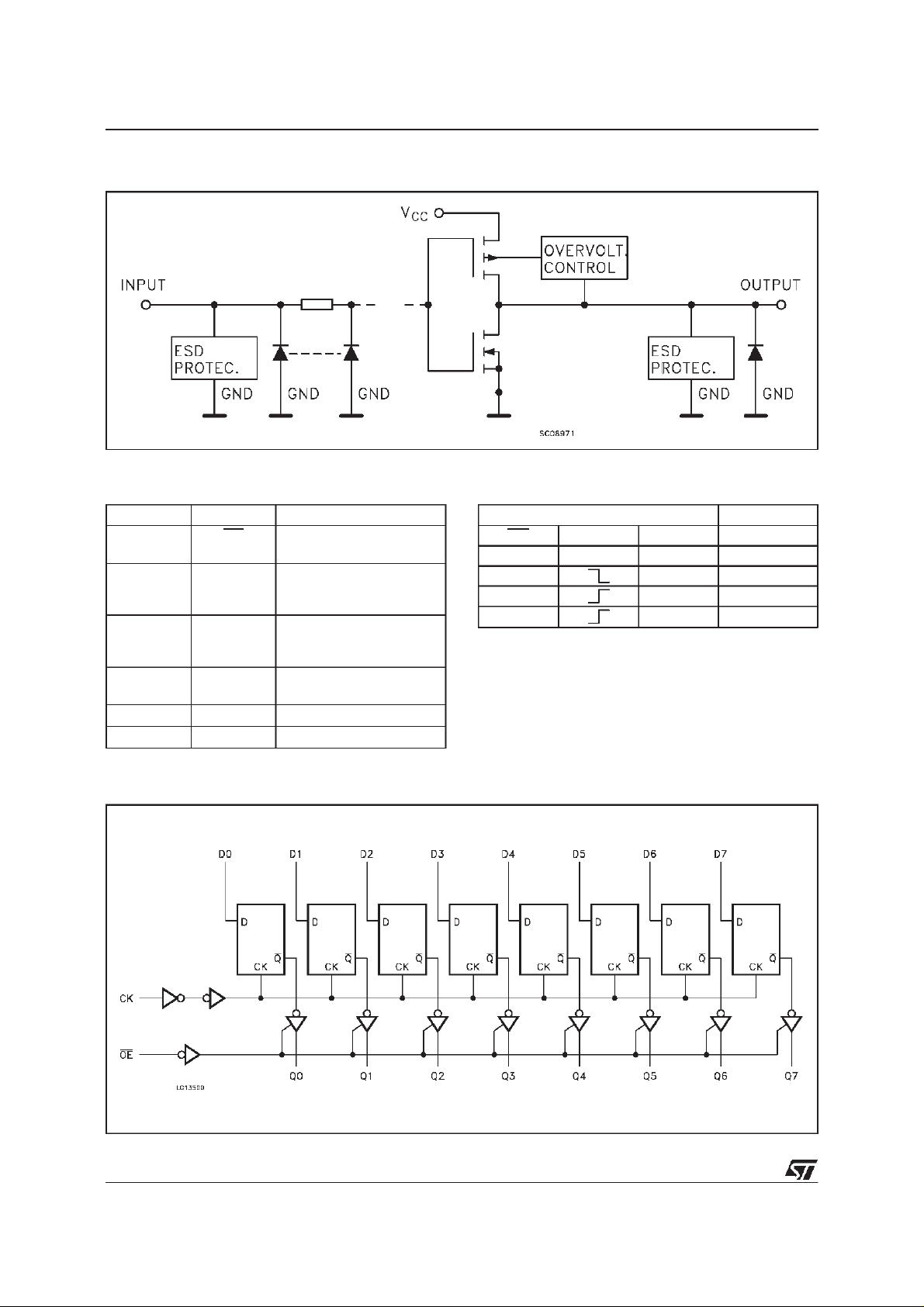
INPUT AND OUTPUTEQUIVALENTCIRCUIT
PIN DESCRIPTION
PI N No SYM B OL NAME AND F U NCTION
1 OE 3 State Output Enable
Input (Active LOW)
2, 5, 6, 9,
12, 15, 16,
19
3, 4, 7, 8,
13, 14, 17,
18
11 CLOCK Clock Input (LOW to
10 GND Ground (0V)
20 V
Q0 to Q7 3 State Outputs
D0 to D7 Data Inputs
HIGH, edge triggered)
CC
Positive Supply Voltage
LOGICDIAGRAM
TRUTH TABLE
INPUTS OUTPUTS
OE CK D Q
HXX Z
L X NO CHANGE
LLL
LHH
X:”H” or”L”
Z: High Impedance
2/10
74LCX374
ABSOLUTE MAXIMUM RATINGS
Symb o l Parameter Val u e Unit
V
V
V
V
I
I
I
I
CC
I
GND
T
T
AbsoluteMaximumRatingsarethosevaluesbeyond whichdamagetothedevicemayoccur.Functionaloperationunderthesecondition isnotimplied.
1)I
absolutemaximum ratingmustbeobserved
O
2)V
<GND, VO>V
O
RECOMMENDED OPERATING CONDITIONS
Supply Voltage -0.5 to + 7.0 V
CC
DC Input Voltage -0.5 to + 7.0 V
I
DC Output Voltage (OFF state) -0.5 to + 7.0 V
O
DC Output Voltage (High or Low State) (note1) -0.5 to VCC+ 0.5 V
O
DC Input Diode Current - 50 mA
IK
DC Output Diode Current (note2)
OK
DC Output Source/Sink Current
O
50 mA
±
50 mA
±
DC Supply Current per Supply Pin ± 100 mA
DC Ground Current per Supply Pin ± 100 mA
Storage Temperature -65 to +150
stg
Lead Temperature (10 sec) 300
L
CC
o
C
o
C
Symb o l Parameter Value Uni t
V
V
V
V
I
OH,IOL
I
OH,IOL
T
dt/dv Input Transition Rise or Fall Rate (V
1)TruthTableguaranteed: 1.5Vto3.6V
2)V
from0.8Vto2.0V
IN
Supply Voltage (note 1) 2.0 to 3.6 V
CC
Input Voltage 0 to 5.5 V
I
Output Voltage (OFF state) 0 to 5.5 V
O
Output Voltage (High or Low State) 0 to V
O
CC
High or Low Level Output Current (VCC= 3.0 to 3.6V) ± 24 mA
High or Low Level Output Current (VCC= 2.7 to 3.0V) ± 12 mA
Operating Temperature: -40 to +85
op
= 3.0V) (note 2) 0 to 10 ns/V
CC
V
o
C
3/10
 Loading...