

SGS Thomson Microelectronics 74LVQ299TTR, 74LVQ299MTR, 74LVQ299M Datasheet
1/12July 2001
■ HIGH SPEED:
t
PD
= 8.3 ns (TYP.) at VCC = 3.3 V
■ COMPATIBLE WITH TTL OU TP U TS
■ LOW POWER DISSIPATION:
I
CC
= 4 µA (MAX.) at TA=25°C
■ LOW NOISE:
V
OLP
= 0.5V (TYP.) at VCC = 3.3V
■ 75Ω TRANSMISSION LINE DRIV ING
CAPABILITY
■ SYMMETRICAL OUTPUT IMPEDANCE:
|I
OH
| = IOL = 12mA (MIN) at VCC = 3.0 V
■ PCI BUS LEVELS GUARANTEED AT 24 mA
■ BALANCED PROPAGATION DELAYS:
t
PLH
≅ t
PHL
■ OPERATING VOLTAGE RANGE:
V
CC
(OPR) = 2V to 3.6V (1.2V Data Retention)
■ PIN AND FUNCTION COMPATIBLE WITH
74 SERIES 299
■ IMPROVED LATCH-UP IMMUNITY
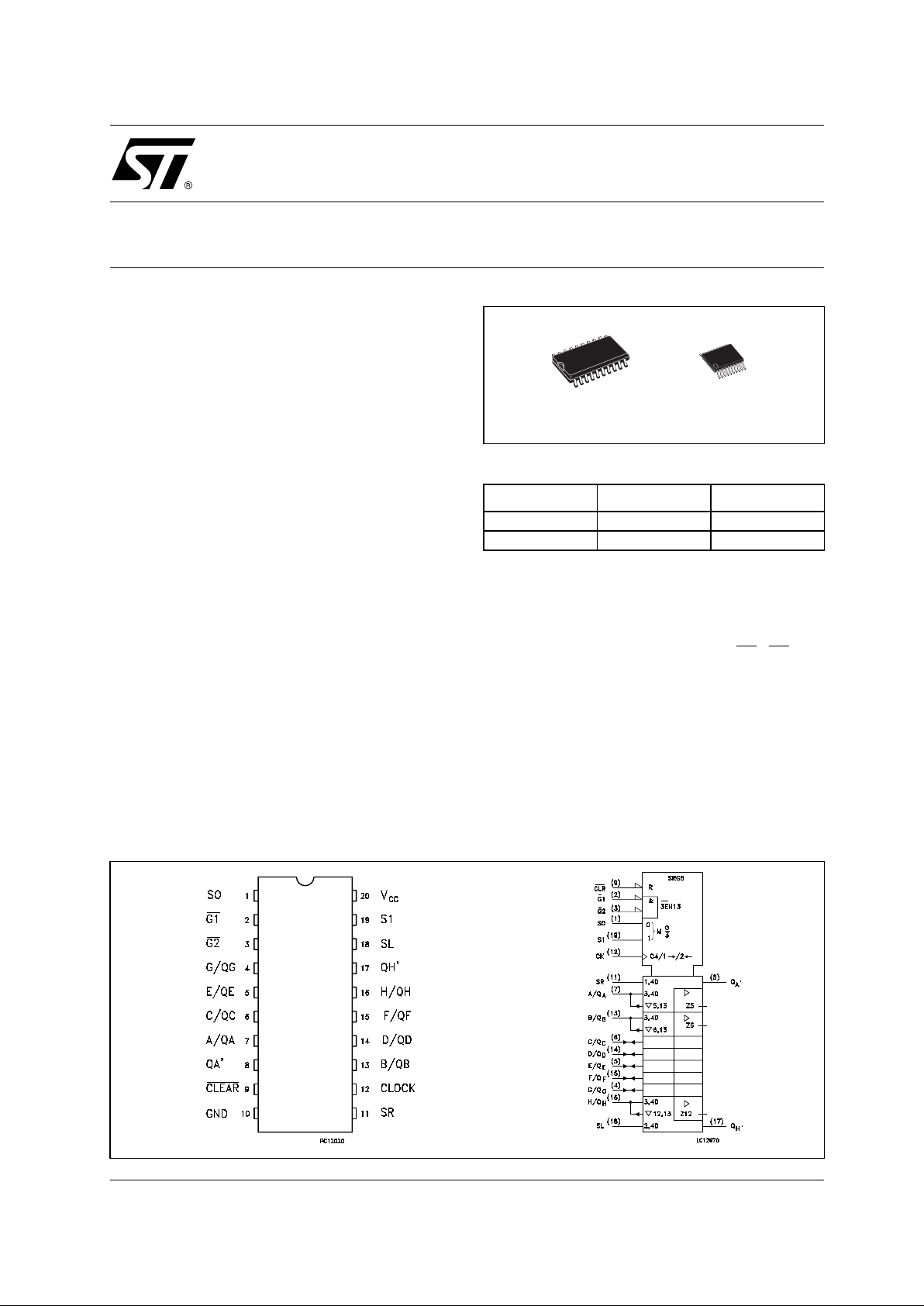
DESCRIPTION
The 74LVQ299 is a low voltage CMOS 8 BIT
PIPO SHIFT REGISTER (3-STATE) fabricated
with sub-micron silicon gate and double-layer
metal wiring C
2
MOS technology. It is ideal for low
power and low noise 3.3V applications.
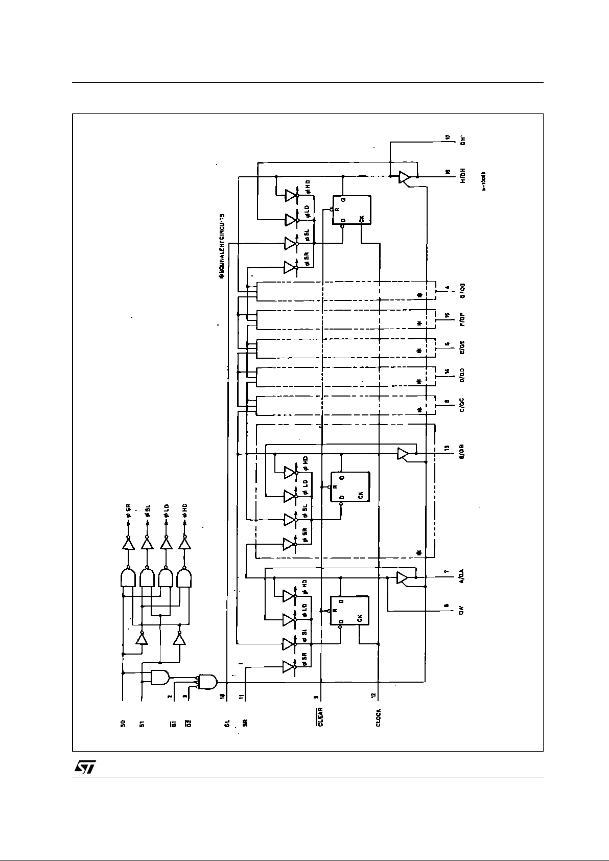
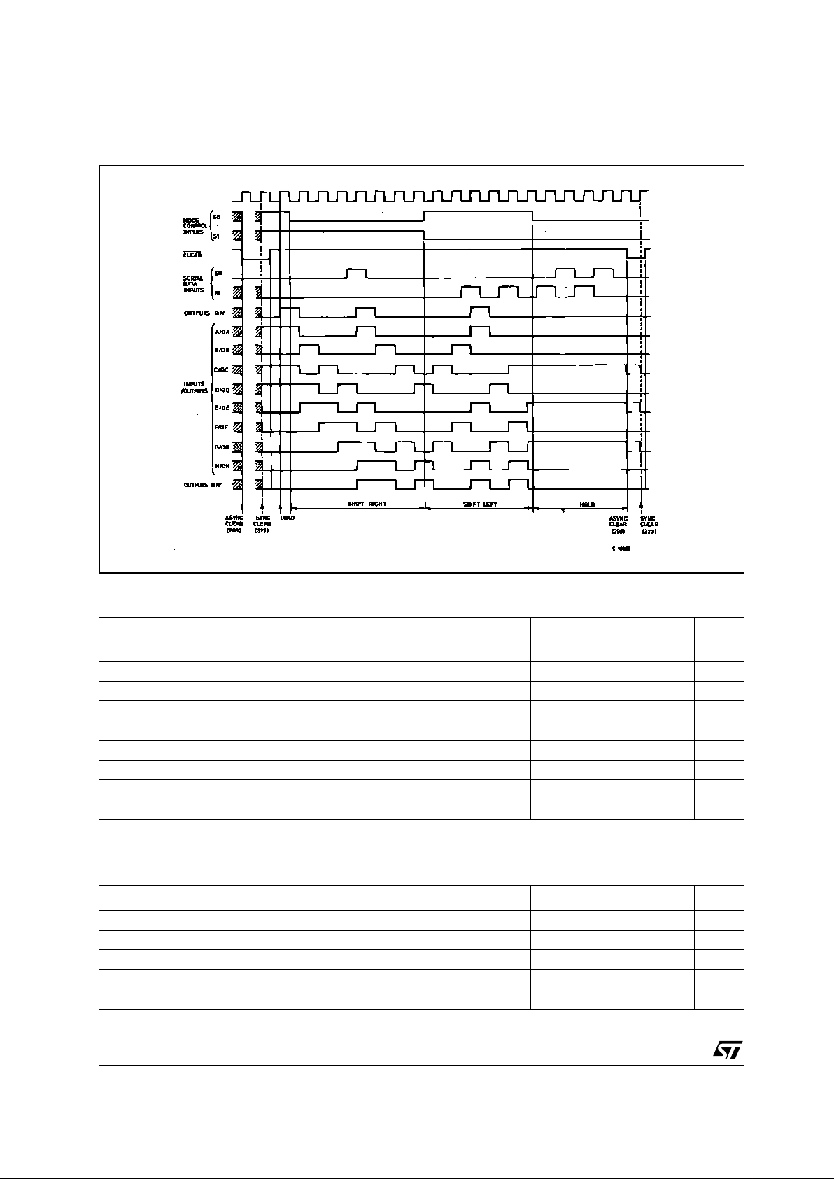
These devices have four modes (HOLD, SHIFT
LEFT, SHIFT RIGHT and LOAD DATA). Each
mode is chosen by tw o fun ction se lect input s (S0,
S1) as shown in the Truth Table.
When one or both enable inputs, (G1
, G2) are
high, the eight input/output terminals are in the
high impedance state; however sequential
operation or clearing of the register is not affected.
Clear function is asynchronous to clock.
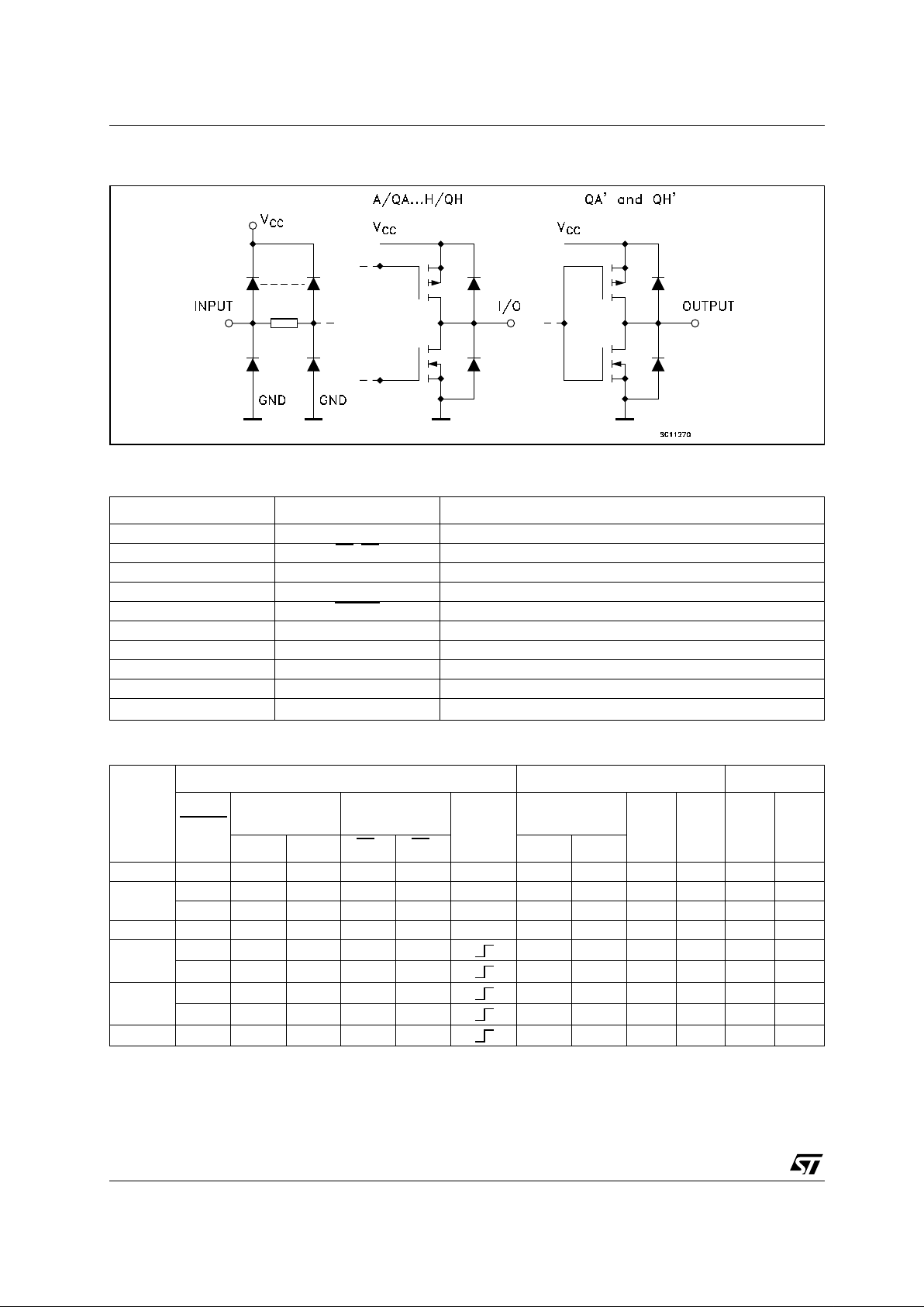
All inputs and outputs are equipped with
protection circuits against stat ic discharge, giving
them 2KV ESD immunity and transient excess
voltage.
74LVQ299
8 BIT PIPO SHIFT REGISTER
WITH ASYNCHRONOUS CLEAR
PIN CONNECTION AND IEC LOGIC SYMBOLS
ORDER CODES
PACKAGE TUBE T & R
SOP 74LVQ299M 74LVQ299MTR
TSSOP 74LVQ299TTR
TSSOPSOP
74LVQ299
2/12
INPUT AND OUTPUT EQUIVALENT CIRCUIT
PIN DESCRIPTION
TRUTH TABLE
* When one or both controls are high, the eight input/output terminals are the high impedance state: however sequential operation or cleaning
of the register is not affected.
Z : High Impedance
Qn0 : The level of An before the indicat ed steady st ate input cond i tions were es tablished.
Qnn : The level of Qn befo re the most recent active tr ansition indicated by OR
a, h : The lev el of the steady s tate inputs A, H, respectiv e l y.
X : Don’t Ca re
PIN No SYMBOL NAME AND FUNCTION
1, 19 S0, S1 Mode Select Inputs
2, 3 G1
, G2 3-State Output Enable Inputs (Active LOW)
7, 13, 6, 14, 5, 15, 4, 16 A/QA to H/QH Parallel Data Inputs or 3-State Parallel Outputs (Bus Driver)
8, 17 QA’,QH’ Serial Outputs (Standard Output)
9 CLEAR
Asynchronous Master Reset Input (Active LOW)
11 SR Serial Data Shift Right Input
12 CLOCK Clock Input (LOW to HIGH, Edge-triggered)
18 SL Serial Data Shift Left Input
10 GND Ground (0V)
20 V
CC
Positive Supply Voltage
MODE
INPUTS INPUTS/OUTPUTS OUTPUTS
CLEAR
FUNCTION
SELECTED
OUTPUT
CONTROL
CLOCK
SERIAL
A/QA H/QH QA’ QH’
S1 S0 G1
*G2*SLSR
ZLHHXXXXXZZLL
CLEAR
L L X L L X X XLLLL
L X L L L X X XLLLL
HOLD H L L L L X X X QA0 QH0 QA0 QH0
SHIFT
RIGHT
H L H L L X H H QGn H QGn
H L H L L X L L QGn L QGn
SHIFT
LEFT
H H L L L H X QBnHQBnH
H H L L L L X QBnLQBnL
LOADH HH X X X Xahah
74LVQ299
3/12
LOGIC DIAGRAM
74LVQ299
4/12
TIMING CHART
ABSOLUTE MAXIMUM RATINGS
Absolute Maximum Ratings are those values beyond which damage to the device may occur. Functional operation under these conditions is
not implied
RECOMMENDED OPERATING CONDITIONS
1) Truth T abl e guarante ed: 1.2V to 3.6 V
2) V
IN
from 0.8V to 2V
Symbol Parameter Value Unit
V
CC
Supply Voltage
-0.5 to +7 V
V
I
DC Input Voltage -0.5 to VCC + 0.5
V
V
O
DC Output Voltage -0.5 to VCC + 0.5
V
I
IK
DC Input Diode Current
± 20 mA
I
OK
DC Output Diode Current
± 20 mA
I
O
DC Output Current
± 50 mA
I
CC
or I
GND
DC VCC or Ground Current
± 400 mA
T
stg
Storage Temperature
-65 to +150 °C
T
L
Lead Temperature (10 sec)
300 °C
Symbol Parameter Value Unit
V
CC
Supply Voltage (note 1)
2 to 3.6 V
V
I
Input Voltage 0 to V
CC
V
V
O
Output Voltage 0 to V
CC
V
T
op
Operating Temperature
-55 to 125 °C
dt/dv
Input Rise and Fall Time V
CC
= 3.0V (note 2)
0 to 10 ns/V
 Loading...