

SGS Thomson Microelectronics 74LVQ273 Datasheet
OCTAL D-TYPE FLIP FLOP WITH CLEAR
■ HIGHSPEED:
=150MHz(TYP.)atVCC=3.3V
f
MAX
■ COMPATIBLEWITHTTLOUTPUT
■
LOW POWERDISSIPATION:
I
=4 µA (MAX.) atTA=25oC
CC
■ LOWNOISE:
=0.4V (TYP.)atVCC=3.3V
V
OLP
■ 75ΩTRANSMISSIONLINEDRIVING
CAPABILITY
■ SYMMETRICALOUTPUTIMPEDANCE:
|I
|=IOL=12 mA (MIN)
OH
■
PCIBUSLEVELSGUARANTEEDAT24mA
■ BALANCEDPROPAGATIONDELAYS:
t
≅ t
PLH
PHL
■ OPERATINGVOLTAGERANGE:
V
(OPR)= 2V to3.6V(1.2VDataRetention)
CC
■
PINANDFUNCTION COMPATIBLEWITH
74SERIES273
■ IMPROVEDLATCH-UPIMMUNITY
DESCRIPTION
The LVQ273 is a low voltage CMOS OCTAL
D-TYPE FLIP FLOP WITH CLEAR fabricated
with sub-micron silicon gate and double-layer
metal wiring C
powerand low noise 3.3V applications.
2
MOS technology. It is ideal for low
74LVQ273
M
(Micro Package)
(TSSOPPackage)
ORDERCODES :
74LVQ273M 74LVQ273T
Information signals applied to D inputs are
transfered to the Q outputs on the positive going
edgeof the clock pulse.
When the CLEAR inputs is held low, the Q
outputs are held low independentelyof the other
inputs.
It has better speed performanceat 3.3V than 5V
LS-TTL family combined with the true CMOS low
powerconsumption.
All inputs and outputs are equipped with
protection circuits against static discharge, giving
them 2KV ESD immunity and transient excess
voltage.
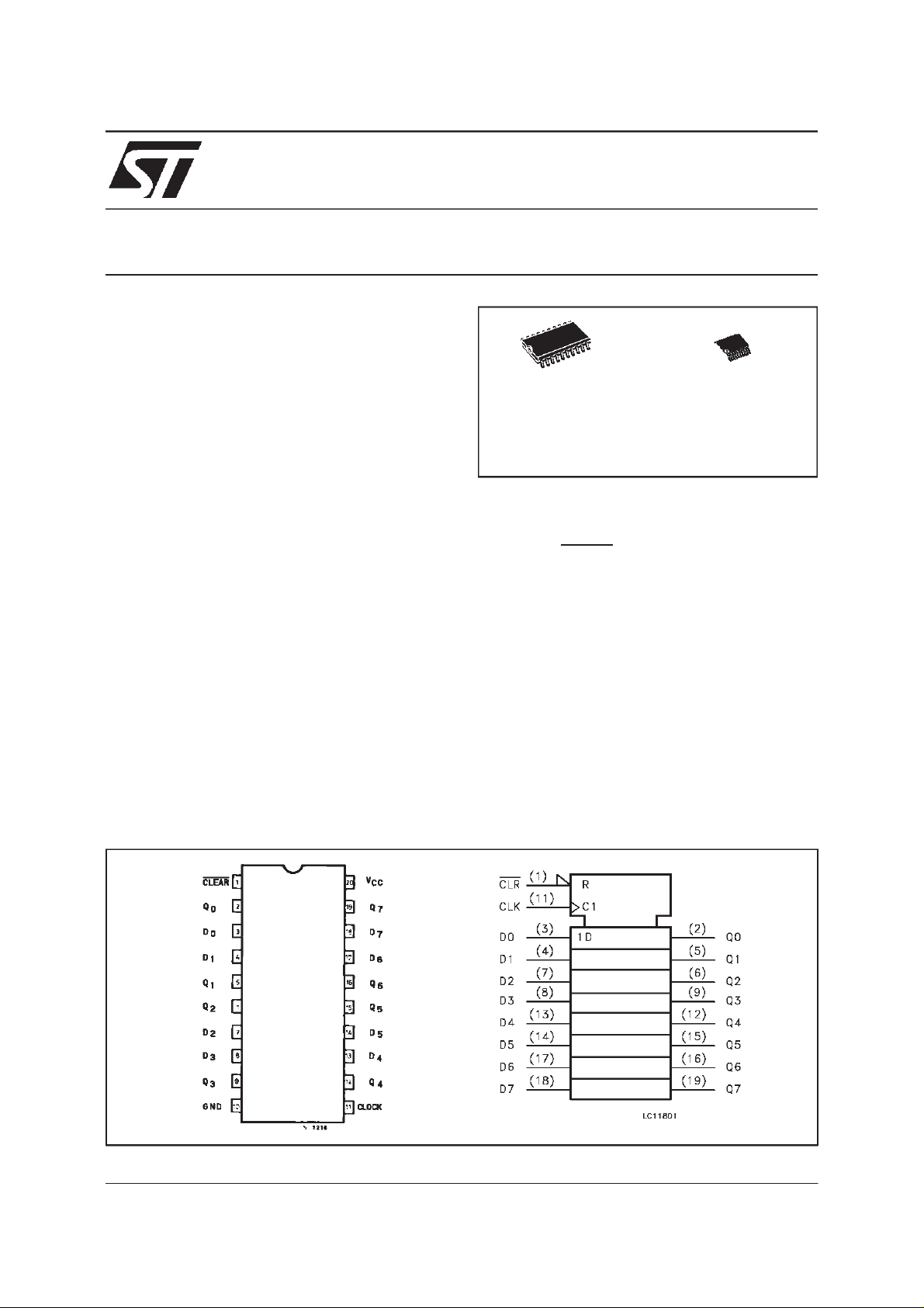
T
PIN CONNECTION AND IEC LOGIC SYMBOLS
February 1999
1/10
74LVQ273
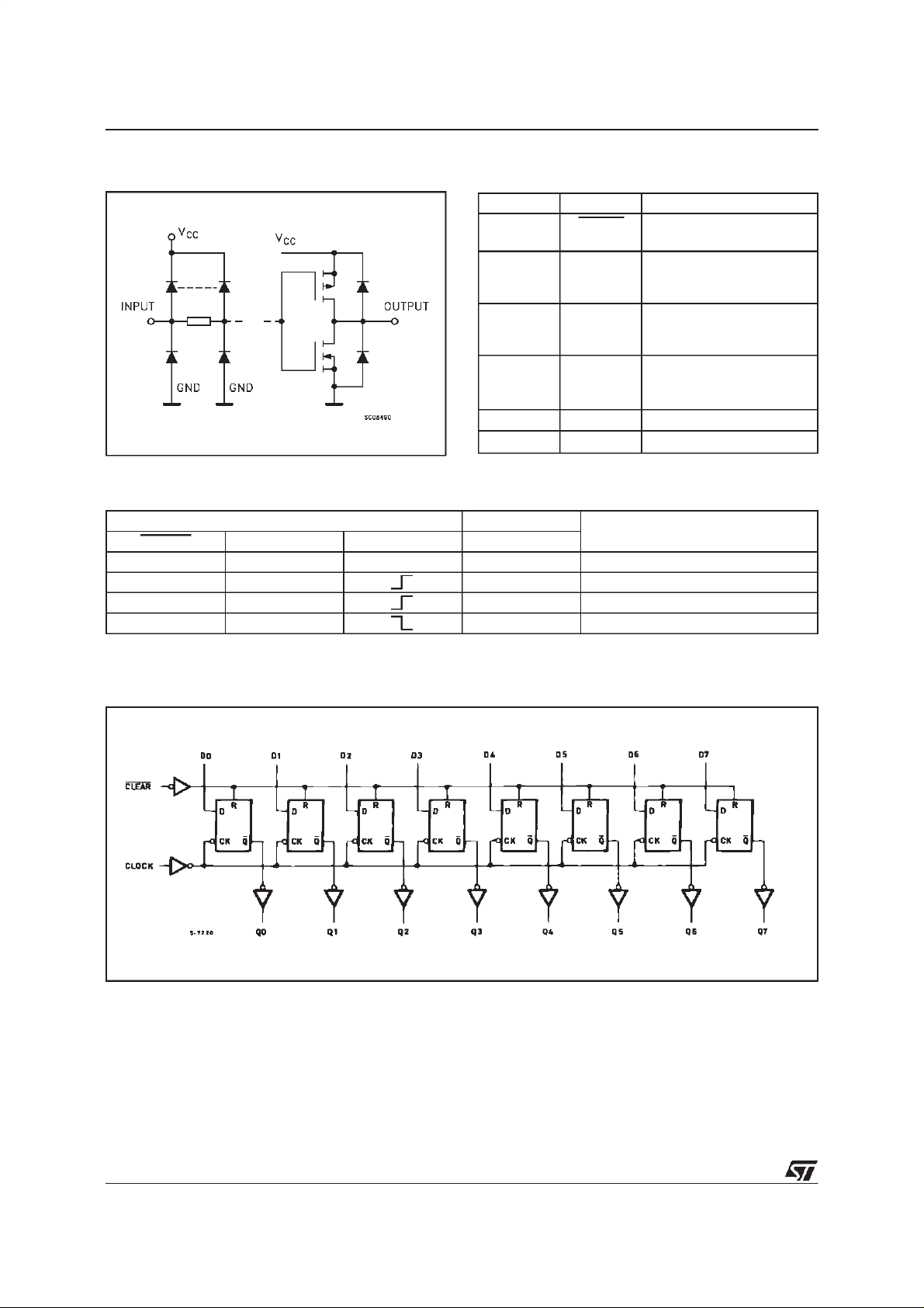
INPUT AND OUTPUT EQUIVALENTCIRCUIT
TRUTH TABLE
INPUTS OUTPUTS FUNCTION
CLE AR D CLOCK Q
L X X L CLEAR
HL L
HH H
HX Q
X:Don’tCare
PIN DESCRIPTION
PI N No SYM BO L NAM E AND F U NCTI ON
1 CLEAR Asyncronous Master
Reset (Active LOW)
2, 5, 6, 9,
12, 15, 16,
19
3, 4, 7, 8,
13, 14, 17,
18
11 CLOCK Clock Input
10 GND Ground (0V)
20 V
n
Q0 to Q7 Flip-Flop Outputs
D0 to D7 Data Inputs
(LOW-to-HIGH, EdgeTriggered)
CC
Positive Supply Voltage
NO CHANGE
LOGICDIAGRAM
Thislogic diagram has not be used to esimate propagation delays
2/10
74LVQ273
ABSOLUTE MAXIMUM RATINGS
Symb o l Para met er Val u e Uni t
V
V
V
I
I
OK
I
or I
I
CC
T
T
AbsoluteMaximumRatingsarethose values beyond whichdamagetothedevicemayoccur.Functionaloperationunderthese conditionisnotimplied.
RECOMMENDED OPERATINGCONDITIONS
Symb o l Para met er Value Un it
V
V
V
T
dt/dv Input Rise and Fall Time (V
1) Truth Table guaranteed: 1.2V to 3.6V
2)V
from0.8Vto 2V
IN
Supply Voltage -0.5 to +7 V
CC
DC Input Voltage -0.5 to VCC+ 0.5 V
I
DC Output Voltage -0.5 to VCC+ 0.5 V
O
DC Input Diode Current ± 20 mA
IK
DC Output Diode Current ± 20 mA
DC Output Current
O
DC VCCor Ground Current
GND
Storage Temperature -65 to +150
stg
Lead Temperature (10 sec) 300
L
Supply Voltage (note 1) 2 to 3.6 V
CC
Input Voltage 0 to V
I
Output Voltage 0 to V
O
Operating Temperature: -40 to +85
op
= 3V) (note 2) 0 to 10 ns/V
CC
50 mA
±
400 mA
±
CC
CC
o
C
o
C
V
V
o
C
3/10
 Loading...