

SGS Thomson Microelectronics 74LVQ245 Datasheet
74LVQ245
LOW VOLTAGE CMOS OCTAL BUS
TRANSCEIVER(3-STATE)
■ HIGHSPEED:t
■
COMPATIBLEWITHTTL OUTPUTS
■ LOW POWERDISSIPATION:
I
=5µA (MAX.) atTA=25oC
CC
■ LOWNOISE:V
■ 75Ω TRANSMISSIONLINEDRIVING
=6 ns(TYP.)atVCC=3.3V
PD
= 0.5V(TYP.)atVCC=3.3V
OLP
CAPABILITY
■ SYMMETRICALOUTPUTIMPEDANCE:
|I
|=IOL=12mA(MIN)
OH
■ PCIBUSLEVELSGUARANTEEDAT 24mA
■ BALANCEDPROPAGATIONDELAYS:
≅
t
t
PLH
PHL
■ OPERATINGVOLTAGERANGE:
V
(OPR)= 2Vto 3.6V (1.2VData Retention)
CC
■ PINANDFUNCTIONCOMPATIBLEWITH
74SERIES245
■
IMPROVEDLATCH-UPIMMUNITY
DESCRIPTION
The LVQ245 is a low voltage CMOS OCTAL BUS
TRANSCEIVER (3-STATE) fabricated with
sub-micron silicon gate and double-layer metal
wiring C
2
MOS technology. It is ideal for low
powerand low noise 3.3V applications.
It has better speed performance at 3.3V than 5V
LSTTL family combined with the true CMOS low
powerconsumption.
M
(Micro Package)
(TSSOPPackage)
T
ORDERCODES :
74LVQ245M 74LVQ245T
This IC is intended for two-way asynchronous
communicationbetween data buses; the direction
of data trasmission is determined by DIR input.
The enable input G can be used to disable the
deviceso thatthe buses are effectivelyisolated.
All inputs and outputs are equipped with
protection circuits against static discharge, giving
them 2KV ESD immunity and transient excess
voltage.
IT IS PROHIBITED TO APPLY A SIGNAL TO A
TERMINAL WHEN IT IS IN OUTPUT MODE
AND WHEN A BUS TERMINAL IS FLOATING
(HIGH IMPEDANCE STATE) IT IS REQUESTED
TO FIX THE INPUT LEVEL BY MEANS OF
EXTERNAL PULL DOWN OR PULL UP
RESISTOR.
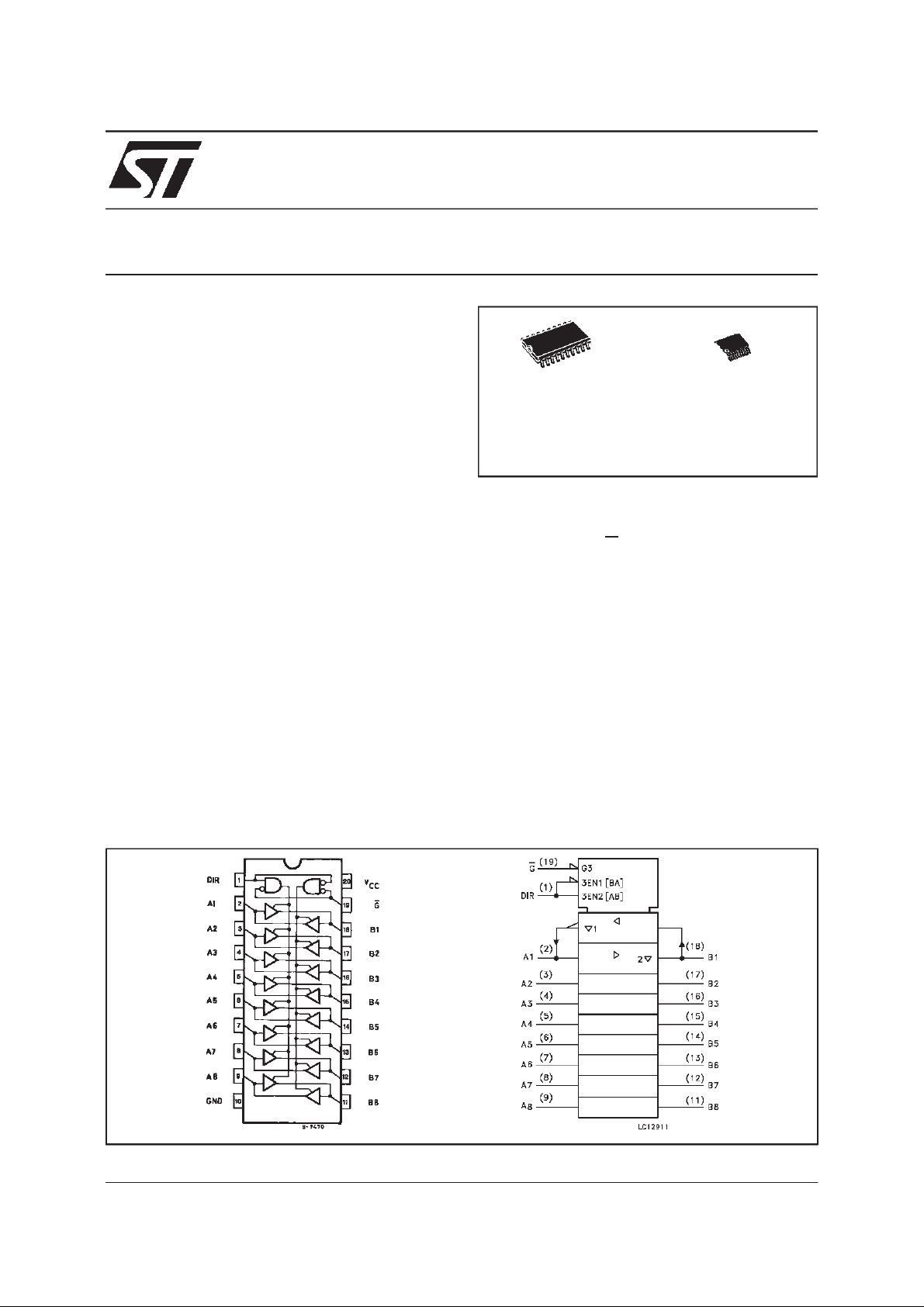
PIN CONNECTIONAND IEC LOGIC SYMBOLS
March 1999
1/8
74LVQ245
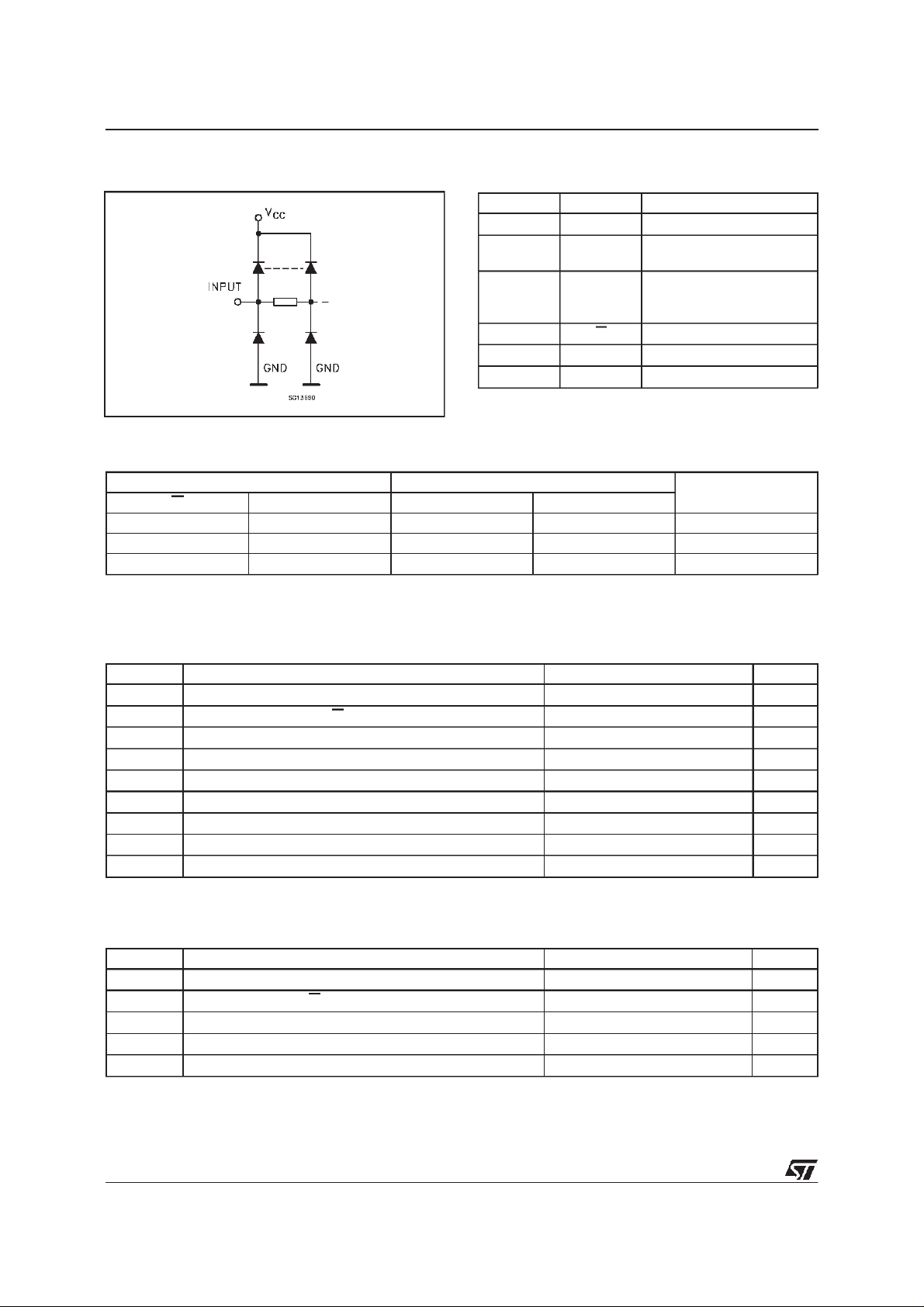
INPUT EQUIVALENTCIRCUIT
TRUTH TABLE
INP UT FUNCTI O N OUT P UT
GDIRABUSBBUS
L L OUTPUT INPUT A = B
L H INPUT OUTPUT B = A
HXZZZ
X:”H” or”L”
Z:Highimpedance
PIN DESCRIPTION
PI N No SYM BO L NAM E AND FUNCTION
1 DIR Directional Control
2, 3, 4, 5,
6, 7, 8, 9
18, 17,16,
15, 14,13,
12, 11
19 G Output Enable Input
10 GND Ground (0V)
20 V
A1 to A8 Data Inputs/Outputs
B1 to B8 Data Inputs/Outputs
CC
Positive Supply Voltage
ABSOLUTE MAXIMUM RATINGS
Symb o l Para met er Val u e Uni t
V
V
V
I
I
OK
I
or I
I
CC
T
T
AbsoluteMaximum Ratingsarethose valuesbeyondwhichdamage tothedevicemayoccur. Functionaloperation underthese condition isnotimplied.
Supply Voltage -0.5 to +7 V
CC
DC Input Voltage (DIR, G) -0.5 to VCC+ 0.5 V
I
DC Bus I/O Voltage -0.5 to VCC+ 0.5 V
I/O
DC Input Diode Current
IK
20 mA
±
DC Output Diode Current ± 20 mA
DC Output Current ± 50 mA
O
DC VCCor Ground Current ± 400 mA
GND
Storage Temperature -65 to +150
stg
Lead Temperature (10 sec) 300
L
o
C
o
C
RECOMMENDEDOPERATINGCONDITIONS
Symb o l Para met er Value Un it
V
V
V
T
t
r,tf
1) Truth Table guaranteed: 1.2V to 3.6V
from0.8Vto2V
2)V
IN
Supply Voltage (note 1) 2 to 3.6 V
CC
Input Voltage (DIR, G) 0 to V
I
Bus I/O Voltage 0 to V
I/O
Operating Temperature: -40 to +85
op
CC
CC
Input Rise and Fall Time (VCC= 3V) (note 2) 0 to 10 ns/V
V
V
o
C
2/8
74LVQ245
DC SPECIFICATIONS
Symbol Parameter Test Conditions Value Unit
T
V
CC
(V)
High Level Input Voltage
V
IH
Low Level Input Voltage 0.8 0.8 V
V
IL
High Level Output
V
OH
3.0 to
3.6
3.0 V
Voltage
Low Level Output
V
OL
3.0 V
Voltage
Input Leakage Current
I
I
3 State Output Leakage
I
OZ
Current
Quiescent Supply
I
CC
3.6
3.6
3.6 VI=VCCor GND 4 40 µA
VO= 0.1V or
-0.1 V
V
CC
(*)
=
IO=-50 µA 2.9 2.99 2.9
I
or
V
IH
V
IL
(*)
I
V
IH
V
IL
=-12 mA 2.58 2.48
I
O
=-24 mA 2.2
I
O
=
IO=50 µA 0.002 0.1 0.1
or
=12 mA 0 0.36 0.44
I
O
=24 mA 0.55
I
O
VI=VCCor GND ±0.1 ±1 µA
VI=VIHor V
IL
VO=VCCor GND
Current
Dynamic Output Current
I
OLD
OHD
(note 1, 2)
I
1) Maximum test duration 2ms,oneoutput loaded attime
2)Incident waveswitchingisguaranteedontransmission lineswithimpedances aslowas 75 Ω.
(*)Alloutputs loaded.
3.6 V
= 0.8 V max 36 mA
OLD
V
= 2 V min -25 mA
OHD
=25oC -40 to 85oC
A
Min. Typ. Max. Min. Max.
2.0 2.0
0.3
±
3
±
µ
V
V
V
A
DYNAMICSWITCHING CHARACTERISTICS
Symbol Parameter Test Conditions Value Unit
T
V
CC
(V)
V
V
V
Dynamic Low Voltage
OLP
Quiet Output (note 1, 2)
OLV
Dynamic High Voltage
IHD
3.3
3.3 2
C
L
=50pF
Input (note 1, 3)
V
Dynamic Low Voltage
ILD
3.3 0.8
Input (note 1, 3)
1)Worstcasepackage
2)Maxnumberofoutputsdefined as(n).Datainputsaredriven 0V to 3.3V,(n -1)outputs switching andoneoutputatGND
3)maxnumberofdatainputs (n)switching.(n-1)switching0Vto3.3V. Inputsunder testswitching:3.3Vto threshold (V
=25oC -40 to 85oC
A
Min. Typ. Max. Min. Max.
0.5 0.8
-0.8 -0.5
),0Vtothreshold (V
ILD
).f=1MHz
IHD
V
3/8
 Loading...