

SGS Thomson Microelectronics 74LVQ20TTR, 74LVQ20MTR, 74LVQ20M Datasheet
74LVQ20
DUAL 4-INPUT NAND GATE
■ HIGH SPEED:
= 5.3 ns (TYP.) at VCC = 3.3 V
t
PD
■ COMPATIBLE WITH TTL OU TP U TS
■ LOW POWER DISSIPATION:
I
= 2µA(MAX.) at TA=25°C
CC
■ LOW NOISE:
= 0.3V (TYP.) at VCC = 3.3V
V
OLP
■ 75Ω TRANSMISSION LINE DRIV ING
CAPABILITY
■ SYMMETRICAL OUTPUT IMPEDANCE:
| = IOL = 12mA (MIN) at VCC = 3.0 V
|I
OH
■ PCI BUS LEVELS GUARANTEED AT 24 mA
■ BALANCED PROPAGATION DELAYS:
≅ t
t
PLH
■ OPERATING VOLTAGE RANGE:
V
CC
■ PIN AND FUNCTION COMPATIBLE WITH
PHL
(OPR) = 2V to 3.6V
74 SERIES 20
■ IMPROVED LATCH-UP IMMUNITY
DESCRIPTION
The 74LVQ20 is a low voltage CMOS DUAL
4-INPUT NAND GATE fabricated with sub-micron
silicon gate and double-layer metal wiring C2MOS
TSSOPSOP
ORDER CODES
PACKAGE TUBE T & R
SOP 74LVQ20M 74LVQ20MTR
TSSOP 74LVQ20TTR
technology. It is ideal for low power and low noise
3.3V applications.
The internal circuit is composed of 3 stages
including buffer output , which enables high noise
immunity and stable output.
All inputs and outputs are equipped with
protection circuits against stat ic discharge, giving
them 2KV ESD immunity and transient excess
voltage.
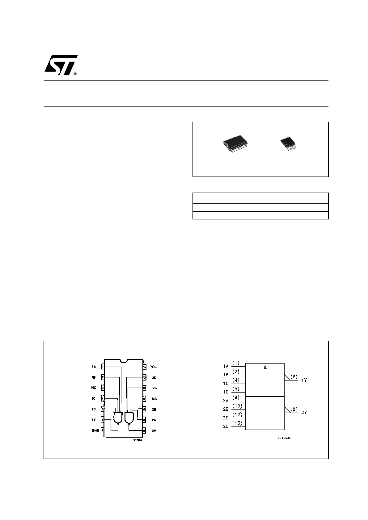
PIN CONNECTION AND IEC LOGIC SYMBOLS
1/8July 2001
74LVQ20
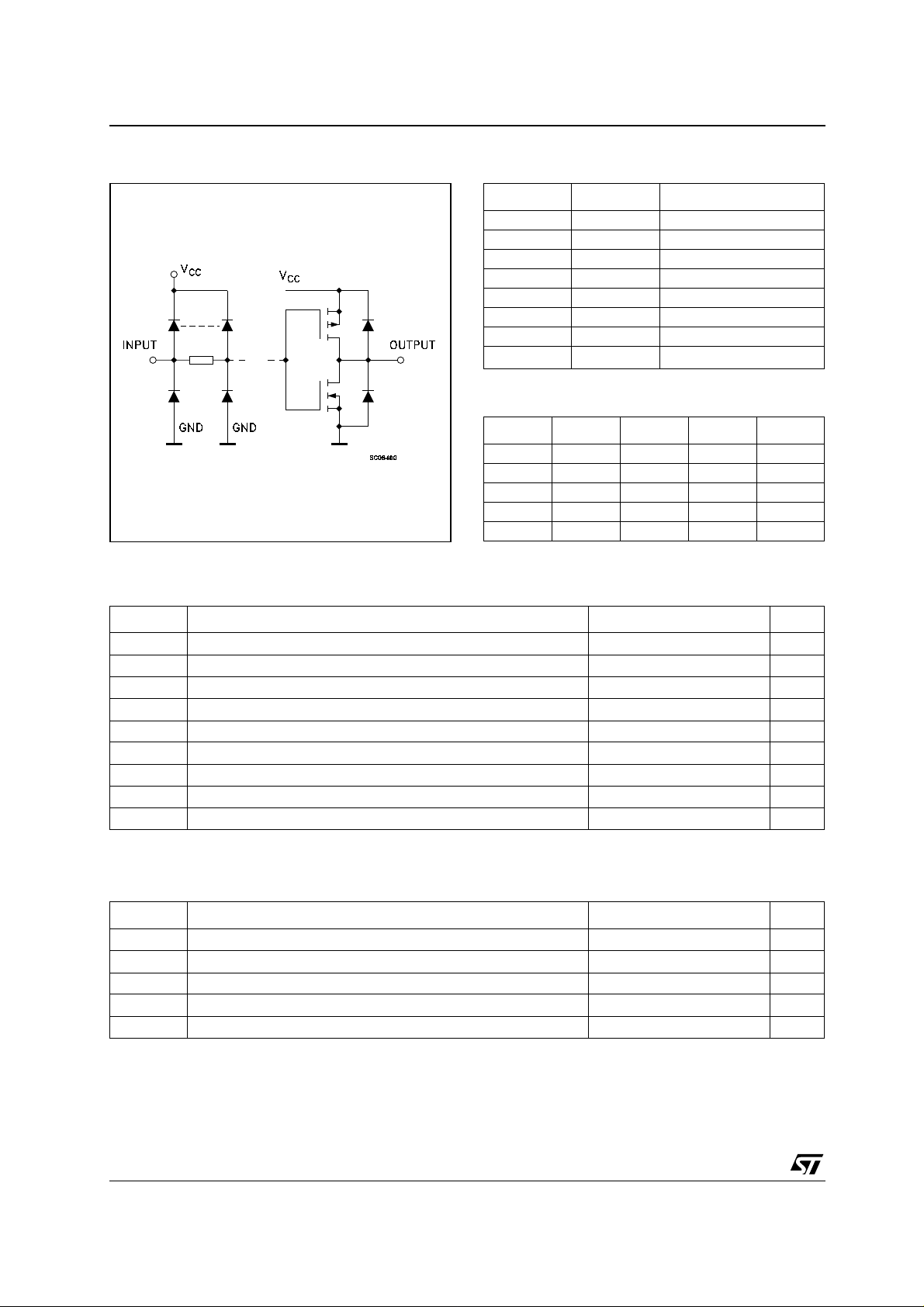
INPUT AND OUTPUT EQUIVALENT CIRCUIT PIN DESCRIPTION
PIN No SYMBOL NAME AND FUNCTION
1, 9 1A to 2A Data Inputs
2, 10 1B to 2B Data Inputs
3, 11 N.C. Not Connected
4, 12 1C to 2C Data Inputs
5, 13 1D to 2D Data Inputs
6, 8 1Y to 2Y Data Outputs
7 GND Ground (0V)
14
TRUTH TABLE
ABCDY
LXXXH
XLXXH
XXLXH
XXXLH
HHHHL
X : Don’t Ca re
V
CC
Positive Supply Voltage
ABSOLUTE MAXIMUM RATINGS
Symbol Parameter Value Unit
V
V
V
I
I
OK
I
I
or I
CC
T
T
Absolute Maximum Ratings are those values beyond which damage to the device may occur. Functional operation under these conditions is
not implied
Supply Voltage
CC
DC Input Voltage -0.5 to VCC + 0.5
I
DC Output Voltage -0.5 to VCC + 0.5
O
DC Input Diode Current
IK
DC Output Diode Current
DC Output Current
O
DC VCC or Ground Current
GND
Storage Temperature
stg
Lead Temperature (10 sec)
L
-0.5 to +7 V
V
V
± 20 mA
± 20 mA
± 50 mA
± 300 mA
-65 to +150 °C
300 °C
RECOMMENDED OPERATING CONDITIONS
Symbol Parameter Value Unit
V
V
V
T
dt/dv
1) Truth T abl e guarante ed: 1.2V to 3.6 V
2) V
from 0.8V to 2V
IN
Supply Voltage (note 1)
CC
Input Voltage 0 to V
I
Output Voltage 0 to V
O
Operating Temperature
op
Input Rise and Fall Time V
= 3.0V (note 2)
CC
2 to 3.6 V
CC
CC
-55 to 125 °C
0 to 10 ns/V
V
V
2/8
DC SPECIFICATIONS
Test Condition Value
T
Symbol Parameter
V
CC
(V)
V
V
V
V
I
I
OLD
I
OHD
1) Maxim um test duration 2ms, one out put loaded at time
2) Incid ent wave sw i tc hi ng is guara nt eed on transmi ssion lines with impedances a s low as 75Ω
High Level Input
IH
Voltage
Low Level Input
IL
Voltage
High Level Output
OH
Voltage
Low Level Output
OL
Voltage
I
Input Leakage
I
Current
Quiescent Supply
CC
Current
Dynamic Output
Current (note 1, 2)
3.0 to
3.6
3.0
3.0
3.6
3.6
3.6
IO=-50 µA
I
=-12 mA
O
I
=-24 mA
O
=50 µA
I
O
I
=12 mA
O
I
=24 mA
O
= VCC or GND
V
I
= VCC or GND
V
I
V
= 0.8 V max
OLD
V
= 2 V min
OHD
= 25°C
A
Min. Typ. Max. Min. Max. Min. Max.
2.0 2.0 2.0 V
0.8 0.8 0.8 V
2.9 2.99 2.9 2.9
2.58 2.48 2.48
0.002 0.1 0.1 0.1
0 0.36 0.44 0.44
± 0.1 ± 1 ± 1 µA
22020µA
74LVQ20
-40 to 85°C -55 to 125°C
2.2 2.2
0.55 0.55
36 25 mA
-25 -25 mA
Unit
V
V
DYNAMIC SWITCHING CHARACTERISTICS
Test Condition Value
T
Symbol Parameter
V
CC
(V)
V
V
V
Dynamic Low
OLP
Voltage Quiet
OLV
Output (note 1, 2)
Dynamic High
IHD
Voltage Input
3.3
3.3 2 V
= 50 pF
C
L
(note 1, 3)
V
ILD
Dynamic Low
Voltage Input
3.3 0.8 V
(note 1, 3)
1) Worst c ase package .
2) Max number of outp ut s defined as (n). Data inputs are driven 0V to 3.3V, (n-1) outputs switching and one output at GND.
3) Max number of data inputs (n) switching. (n-1) switching 0V to 3.3V. Inputs under test switching: 3.3V to threshold (V
(V
), f=1MHz.
IHD
= 25°C
A
-40 to 85°C -55 to 125°C
Min. Typ. Max. Min. Max. Min. Max.
0.3 0.8
-0.8 -0.3
ILD
Unit
V
), 0V to threshold
3/8
 Loading...