

SGS Thomson Microelectronics 74LVQ14 Datasheet
74LVQ14
HEX SCHMITT INVERTER
■ HIGHSPEED:t
■
COMPATIBLEWITHTTLOUTPUTS
■ LOW POWERDISSIPATION:
I
=2µA (MAX.)at TA=25oC
CC
■ LOWNOISE:
V
=0.3 V (TYP.)at VCC=3.3V
OLP
■
75ΩTRANSMISSIONLINEDRIVING
=6 ns(TYP.)atVCC=3.3V
PD
CAPABILITY
■ SYMMETRICALOUTPUTIMPEDANCE:
|I
|=IOL=12mA(MIN)
OH
■ PCIBUSLEVELSGUARANTEEDAT 24mA
■
BALANCEDPROPAGAT IONDELAYS:
t
≅ t
PLH
PHL
■ OPERATINGVOLTAGERANGE:
V
(OPR)= 2Vto3.6V
CC
■ PINANDFUNCTION COMPATIBLEWITH
74SERIES14
■ IMPROVEDLATCH-UP IMMUNITY
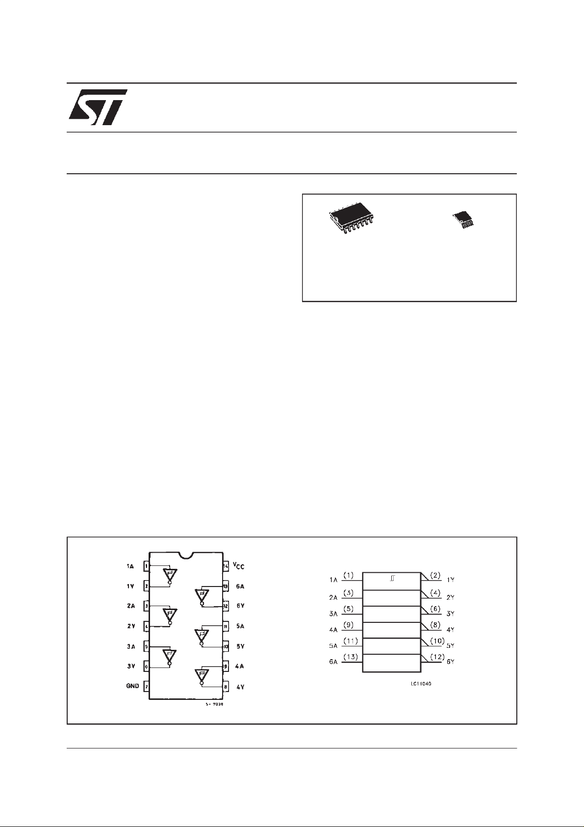
DESCRIPTION
The LVQ14 is a low voltage CMOS HEX
SCHMITT INVERTER fabricated with sub-micron
silicon gate and double-layermetal wiring C
2
MOS
technology.Itis ideal for low power and low noise
3.3Vapplications.
The internal circuit is composed of 3 stages
M
(Micro Package)
(TSSOPPackage)
T
ORDERCODES :
74LVQ14M 74LVQ14T
including buffer output, which enables high noise
immunityand stable output.
It has better speed performanceat 3.3V than 5V
lsttl family combined with the true CMOS low
powerconsumption.
Pin configuration and function are the same as
thoseof the LVQ04 but the LVQ14has hysteresis
betweenthe positiveand negative input threshold
typicallyof 1V.
This together with its schmitt trigger function
allows it to be used on line receivers with slow
rise/fallinputsignals.
All inputs and outputs are equipped with
protection circuits against static discharge, giving
them 2KV ESD immunity and transient excess
voltage.
PIN CONNECTION AND IEC LOGIC SYMBOLS
February 1999
1/8
74LVQ14
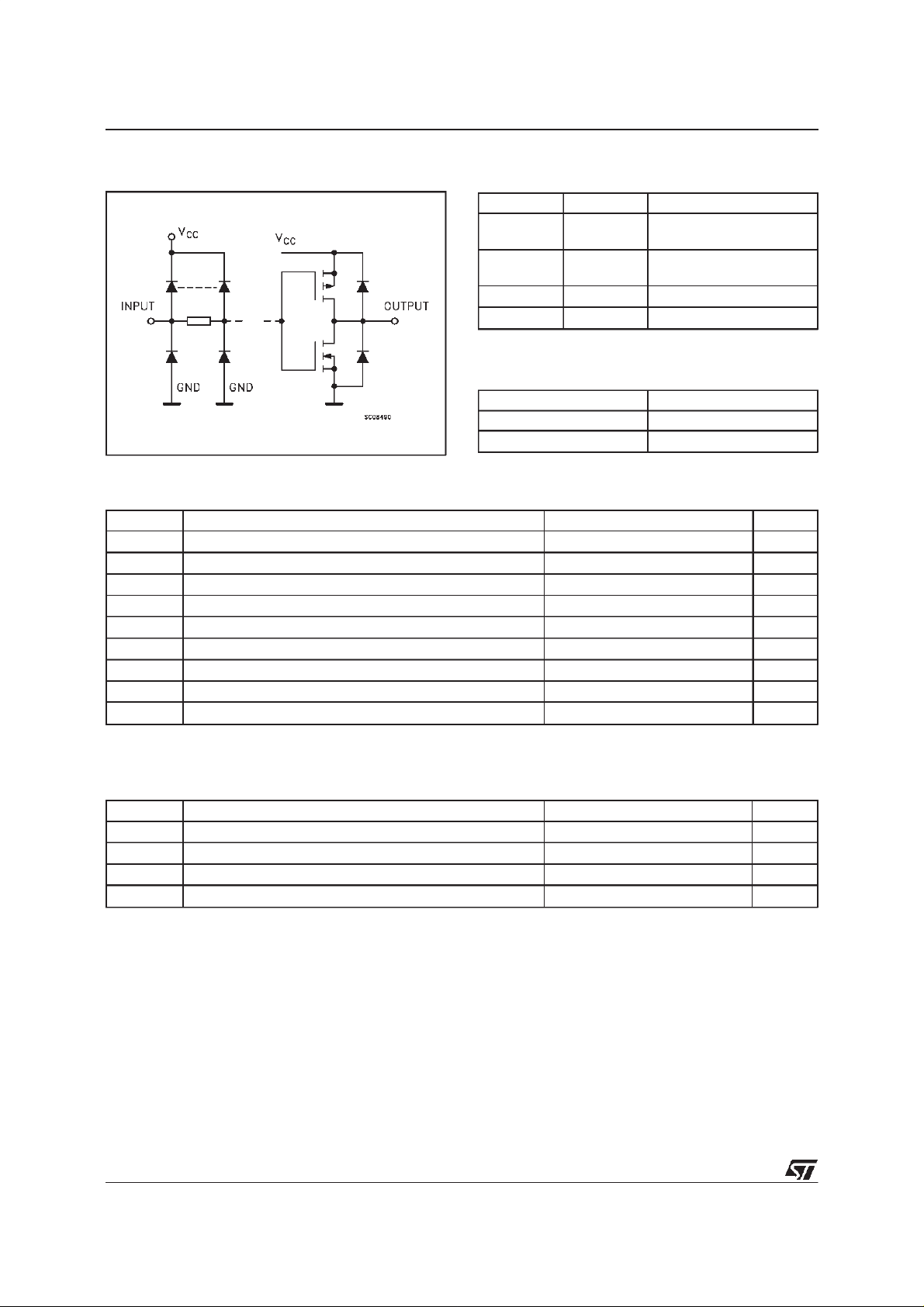
INPUT AND OUTPUTEQUIVALENT CIRCUIT
PIN DESCRIPTION
PI N No SYMB OL NAME AND FU NCTION
1, 3, 5, 9,
1A to 6A Data Inputs
11, 13
2, 4, 6, 8,
1Y to 6Y Data Outputs
10, 12
7 GND Ground (0V)
14 V
CC
Positive Supply Voltage
TRUTH TABLE
AY
LH
HL
ABSOLUTE MAXIMUM RATINGS
Symb o l Para met er Val u e Uni t
V
V
V
I
I
OK
I
or I
I
CC
T
T
AbsoluteMaximumRatingsarethosevaluesbeyond whichdamagetothedevice mayoccur. Functionaloperationunderthesecondition isnotimplied.
Supply Voltage -0.5 to +7 V
CC
DC Input Voltage -0.5 to VCC+ 0.5 V
I
DC Output Voltage -0.5 to VCC+ 0.5 V
O
DC Input Diode Current
IK
DC Output Diode Current
DC Output Current ± 50 mA
O
DC VCCor Ground Current ± 300 mA
GND
Storage Temperature -65 to +150
stg
Lead Temperature (10 sec) 300
L
20 mA
±
20 mA
±
o
C
o
C
RECOMMENDED OPERATINGCONDITIONS
Symb o l Para met er Value Un it
V
V
V
T
1) TruthTable guaranteed: 1.5Vto3.6V
2/8
Supply Voltage (note 1) 2 to 3.6 V
CC
Input Voltage 0 to V
I
Output Voltage 0 to V
O
Operating Temperature: -40 to +85
op
CC
CC
V
V
o
C
74LVQ14
DC SPECIFICATIONS
Symbol Parameter Test Conditions Value Unit
T
V
CC
(V)
Positive Input Threshold
V
t+
Negative Input Threshold 3.0 0.9 0.9 V
V
t-
Hysteresis Voltage 3.0 0.3 1.2 0.3 1.2 V
V
H
High Level Output
V
OH
Voltage
Low Level Output
V
OL
Voltage
Input Leakage Current
I
I
Quiescent Supply
I
CC
3.0
3.0
3.0
3.6
V
V
IO=-50µA 2.9 2.99 2.9
(*)
=
I
V
IL
(*)
I
V
IH
=-12 mA 2.58 2.48
I
O
=-24 mA 2.2
I
O
IO=50 µA 0.002 0.1 0.1
=
=12 mA 0 0.36 0.44
I
O
=24 mA 0.55
I
O
VI=VCCor GND
3.6 VI=VCCor GND 2 20
Current
Dynamic Output Current
I
OLD
OHD
(note 1, 2)
I
1) Maximumtest duration 2ms, one output loaded attime
2)Incident waveswitchingisguaranteed ontransmission lines withimpedances aslowas50 Ω.
(*)All outputs loaded.
3.6 V
= 0.8 V max 36 mA
OLD
V
= 2 V min -25 mA
OHD
=25oC -40 t o 85oC
A
Min. Typ. Max. Min. Max.
2.2 2.2
0.1
±
1
±
µ
µ
V
V
V
A
A
DYNAMICSWITCHING CHARACTERISTICS
Symbol Parameter Test Conditions Value Unit
T
V
CC
(V)
V
V
V
Dynamic Low Voltage
OLP
Quiet Output (note 1, 2)
OLV
Dynamic High Voltage
IHD
3.3
3.3 2
C
L
=50pF
Input (note 1, 3)
V
Dynamic Low Voltage
ILD
3.3 0.8
Input (note 1, 3)
1)Worstcasepackage.
2)Maxnumberofoutputsdefined as(n).Datainputs aredriven0Vto3.3V,(n -1)outputs switchingandoneoutput atGND.
3)Maxnumberofdatainputs (n)switching.(n-1)switching0Vto3.3V.Inputs undertestswitching: 3.3Vtothreshold (V
=25oC -40 t o 85oC
A
Min. Typ. Max. Min. Max.
0.3 0.8
-0.8 -0.3
),0Vtothreshold(V
ILD
).,f=1MHz.
IHD
V
3/8
 Loading...