1/9February 2002
■ 5V TOLERANT INPUTS
■ HIGH SPEED: t
PD
= 4.2ns (MAX.) at VCC = 3V
■ POWER DOWN PROTECTION ON INPU T S
AND OUTPUTS
■ SYMMETRICAL OUTPUT IMPEDANCE:
|I
OH
| = IOL = 24mA (MIN) at VCC = 3V
■ PCI BUS LEVELS GUARANT EED AT 2 4 mA
■ BALANCED PROPAGATION DELAYS:
t
PLH
≅ t
PHL
■
OPERATING VOLTAGE RANGE:
V
CC
(OPR) = 1.65V to 3.6V (1.2V Data
Retention)
■ PIN AND FUNCTION COMPATIBLE WITH
74 SERIES 541
■ LATCH-UP PERFORMANCE EXCEEDS
500mA (JESD 17)
■ ESD PERFORMANCE:
HBM > 2000V (MIL STD 883 method 3015);
MM > 200V
DESCRIPTION
The 74LVC541A is a lo w voltage CMOS OCTAL
BUS BUFFER (3-STATE) fabricated with
sub-micron silicon gate and double-layer metal
wiring C
2
MOS tecnology. It is ideal fo r 1.6 5 to 3. 6
V
CC
operations and low power and low noise
applications.
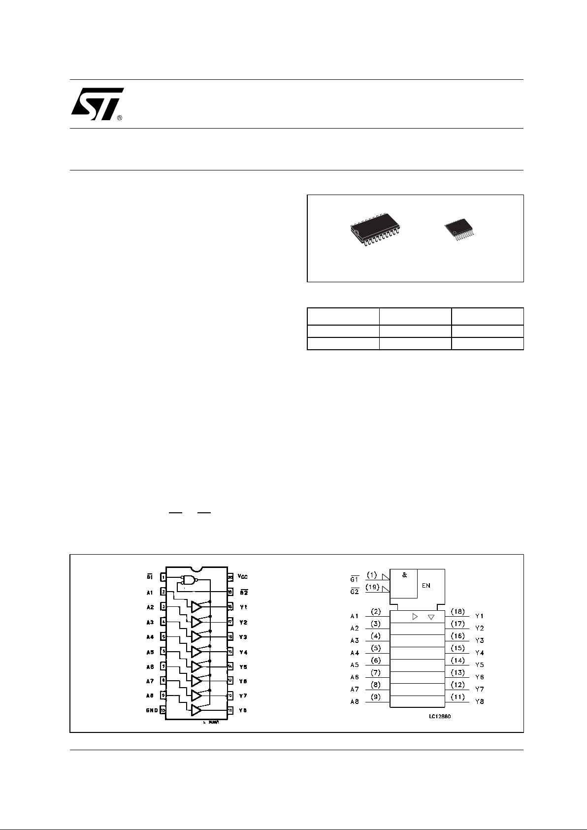
The 3 STATE control gate opera tes as two input
AND such that if either G1
or G2 are high, all eight
outputs are in the high impedance state.
In order to enhance PC board layout, the
74LVC541A offers a pinout having inputs and
outputs on opposite sides of the package.
This device is designed to interface di rectly High
Speed CMOS systems with TTL and NMOS
components.
It has more speed performance at 3.3V than 5V
AC/ACT family, combined with a lower power
consumption.
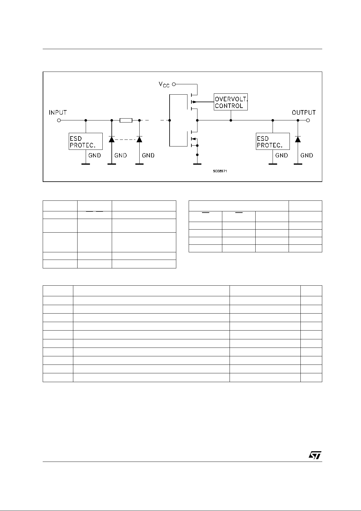
All inputs are equipped with protection circuits
against static discharge, giving them 2KV ESD
immunity and transient excess voltage.
74LVC541A
OCTAL D-TYPE LATCH
HIGH PERFORMANCE
This is preliminary information on a new product now in development are or undergoing evaluation. Details subject to change without notice.
PIN CONNECTION AND IEC LOGIC SYMBOLS
ORDER CODES
PACKAGE TUBE T & R
SOP 74LVC541AM 74LVC541AMTR
TSSOP 74LVC541ATTR
TSSOPSOP
PRELIMINARY DATA

74LVC541A
2/9
INPUT AND OUTPUT EQUIVALENT CIRCUIT
PIN DESCRIPTION TRUTH TABLE
X=Don ’ t c are; Z=High Impedance
ABSOLUTE MAXIMUM RATINGS
Absolute Maximum Rating are t hose value beyond which damage to the device ma y occour . Functional ope rat i on unde r these condition is
not implied
1) I
O
absolute ma xim um rating must be obse rved
2) V
O
< GND, VO > V
CC
PIN No SYMBOL NAME AND FUNCTION
1, 19 G1
, G2 Output Enable Inputs
2, 3, 4, 5, 6,
7, 8, 9
A1 to A8 Data Inputs
18, 17, 16,
15, 14, 13,
12, 11
Y1 to Y8 Data Outputs
10 GND Ground (0V)
20 V
CC
Positive Supply Voltage
INPUT OUTPUT
G1
G2 An Yn
HXXZ
XHXZ
LLHH
LLLL
Symbol Parameter² Value Unit
V
CC
Supply Voltage
-0.5 to +7.0 V
V
I
DC Input Voltage
-0.5 to +7.0 V
V
O
DC Output Voltage (VCC = 0V)
-0.5 to +7.0 V
V
O
DC Output Voltage (High or Low State) (note 1) -0.5 to VCC + 0.5
V
I
IK
DC Input Diode Current
- 50 mA
I
OK
DC Output Diode Current (note 2)
- 50 mA
I
O
DC Output Current
± 50 mA
I
CC
or I
GND
DC VCC or Ground Current per Supply Pin
± 100 mA
T
stg
Storage Temperature
-65 to +150 °C
T
L
Lead Temperature (10 sec)
300 °C

74LVC541A
3/9
RECOMMENDED OPERATING CONDITIONS
1) Truth T abl e guarante ed: 1.2V to 3.6 V
2) V
IN
from 0.8V to 2V at VCC = 3.0V
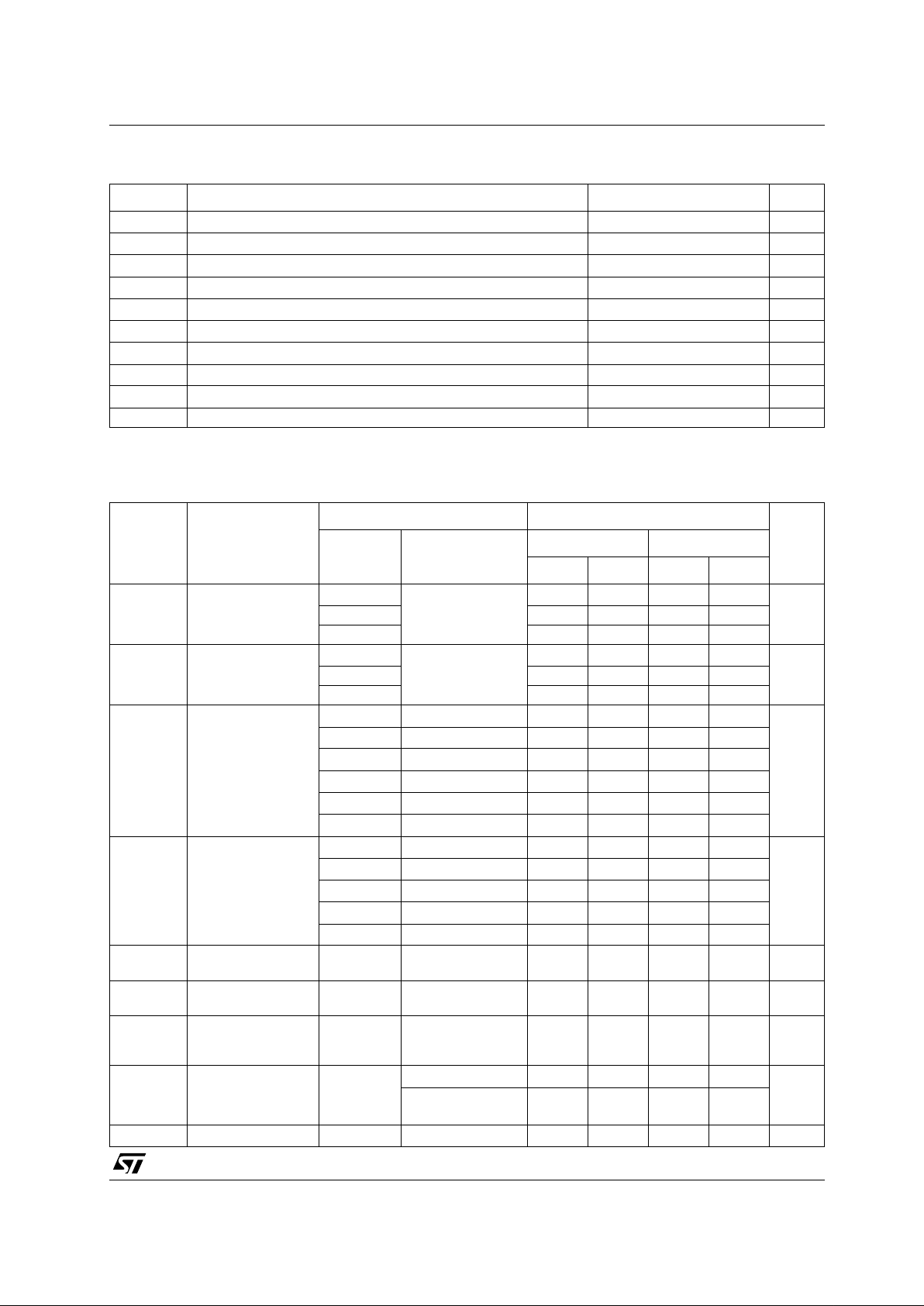
DC SPECIFICATION
Symbol Parameter Value Unit
V
CC
Supply Voltage (note 1)
1.65 to 3.6 V
V
I
Input Voltage
0 to 5.5 V
V
O
Output Voltage (VCC = 0V)
0 to 5.5 V
V
O
Output Voltage (High or Low State) 0 to V
CC
V
I
OH
, I
OL
High or Low Level Output Current (VCC = 3.0 to 3.6V)
± 24 mA
I
OH
, I
OL
High or Low Level Output Current (VCC = 2.7 to 3.0V)
± 12 mA
I
OH
, I
OL
High or Low Level Output Current (VCC = 2.3 to 2.7V)
± 8mA
I
OH
, I
OL
High or Low Level Output Current (VCC = 1.65 to 2.3V)
± 4mA
T
op
Operating Temperqture
-40 to 85 °C
dt/dv Input Rise and Fall Time (note 2) 0 to 10 ns/V
Symbol Parameter
Test Condition Value
Unit
V
CC
(V)
-40 to 85 °C -55 to 125 °C
Min. Max. Min. Max.
V
IH
High Level Input
Voltage
1.65 to 1.95
0.65V
CC
0.65V
CC
V
2.3 to 2.7 1.7 1.7
2.7 to 3.6 2 2
V
IL
Low Level Input
Voltage
1.65 to 1.95
0.35V
CC
0.35V
CC
V
2.3 to 2.7 0.7 0.7
2.7 to 3.6 0.8 0.8
V
OH
High Level Ouput
Voltage
1.65 to 3.6
IO=-100 µAVCC-0.2 VCC-0.2
V
1.65
I
O
=-4 mA
1.2 1.2
2.3
I
O
=-8 mA
1.7 1.7
2.7
I
O
=-12 mA
2.2 2.2
3.0
I
O
=-18 mA
2.4 2.4
3.0
I
O
=-24 mA
2.2 2.2
V
OL
Low Level Output
Voltage
1.65 to 3.6
I
O
=100 µA
0.2 0.2
V
1.65
I
O
=4 mA
0.45 0.45
2.3
I
O
=8 mA
0.7 0.7
2.7
I
O
=12 mA
0.4 0.4
3.0
I
O
=24 mA
0.55 0.55
I
I
Input Leakage
Current
3.6
V
I
= 0 to 5.5V
± 5 ± 5 µA
I
off
Power Off Leakage
Current
0
V
I
or VO = 5.5V
100 100 µA
I
OZ
High Impedance
Output Leakage
Current
3.6 VI = VIH orVIL
V
O
= 0 to 5.5V
± 5 ± 5 µA
I
CC
Quiescent Supply
Current
3.6
VI = VCC or GND
10 10
µA
V
I
or VO = 3.6 to
5.5V
± 10 ± 10
∆I
CC
ICC incr. per Input
2.7 to 3.6
VIH = VCC-0.6V
500 500 µA
 Loading...